This thread has been locked.

If you have a related question, please click the "Ask a related question" button in the top right corner. The newly created question will be automatically linked to this question.

DAC088S085: [DAC088S085] Dout data inverted ?

Part Number: DAC088S085
Other Parts Discussed in Thread: LM3409

Hello,

I try to make 3 DAC088S085 working in daisy chain mode.
I am able to make the first 2 IC working with good analog outputs but the third one does not work even in WRM or WTM.

What I can see on scope is that at the first IC DIN and DOUT are out of phase for about 90°. Here is my mesurement :

Top channel is the input from MOSI, second is SCLK and third id the IC's DOUT. Is that normal?
So taht the first IC is sampling data on falling edges of SCLK but others (second and third) are sampling on rising edge.

I tried replacing all IC, checking soldering (these are WQFN packages). I tried removing IC #2 and #3 but same result.

Any idea ? Thanks.

Serge

  • Hi,

    Can you please post your schematics of  daisy chain implementation?

    As I can see from the scope shot, its not inverted, just a bit shift.

    Please include DIN and DOUT of the first DAC and DOUT of the second DAC for clarity.

    Regards,

    AK

  • Thanks for your answer. The data shift looks bigger enough to change the SCK sampling.

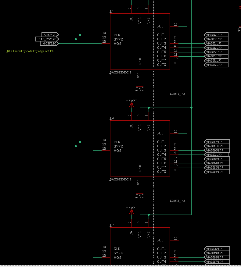
    I tried to make images you requested, but it is relly not easy. Here is the schematic, it is actually a copy paste of the documentation in term of connections. References voltages are 1.5V and supply 3.3V

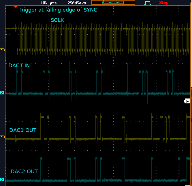
    Here is the scope screenshots. All waveforms are synced with SYNC falling edge.

    I tied to reduce the frame length from 6 bytes to 4 bytes. DAC1 & 2 still continue to work but not #3. Tried also to send 8 bytes but nothing more.

    Spent 3 days on this double checking every things but no clue at all (but this out of phase data).

    An idea on what I should observe on the 3rd DAC output even if not connected?

    Serge.

  • Hello,

    I can see today that there is no more shift between SCK and Dout when the idle state of clock is LOW (but in this case data samplig occurs on rising edge).
    Since signals are fed through LVDS receivers I tried to invert the input pair to invert clock but no way to make it working.

    I'm using a SPI device in a Zynq processor from a Xilinx FPGA. I tried all availables modes but none acheive the DAC requirement.
    I don't know if the FPGA or DAC out of SPI sepcifications (or maybe my way of working with it).

    Is there a example using Zynq for this DAC or another Zynq compatible SPI daisy chained IC DAC I can use?

    The only way I can see is to make my own master SPI using bitbanging in VHDL or using another IC.

    Any idea? Thanks.

    Serge.

  • Hi,

    Your scope shot show's that DAC2_OUT is correct as per DIN you entered. So I wont see any problem with the  interface. I am assuming you are giving 48 clock pulses.

    Please note that in daisy chain config, DOUT1 remains low for the first fourteen falling edges of SCLK before going high on the fifteenth falling edge.  subsequently, the next sixteen falling edges of SCLK outputs the first sixteen data bits entered into DIN. similarly for DUT2, 15th and 31st clock edge.

    what is the output you are observing on DAC3? As a debug, Can you send all 1's to DAC3 through daisy chain and observe the output?

    We don't have any example code in VHDL or C for this part, but I will help you with this debug.

    Regards,

    AK

  • Hello, thanks for your help.

    Everything is now working my problem was probably due to a bad solder on a VCC pad.

    Here are 2 screenshots where from bottom to top : DAC1 DIN, SCLK, DAC1 DOUT and DAC2 DOUT
    the first one with clock phase = 0 (DAC1 sampling input data at falling edge of clock but DAC2 sampling at rising edge)
    and clock phase = 1 for the second image (DAC1 & 2 sampling data at rising edge of clock).
    Both configurations are working (I suppose I must use the first?).

    This setting is used on a big board of about 380mm x 60mm (120mm between DAC).
    These 24 analog outputs will feed 24 LM3409 buck current controllers (on their current adjust pins).
    So the board will be very noisy, any advice on what to add to avoid glitches on data lines?

    greetings from France, have a nice day.

    Serge

  • Hi,

    Are you using these for power supply margining or current limit adjust?

    Anyway happy to know that your problem got solved.

    If you need to avoid glitches in the data lines of the DAC, I need to really look into the layout. for quick, you can add series termination resistors on the SPI interface to reduce the edge rate and have an unbroken ground plane below these digital lines for the return current to follow,

    Regards,

    AK

  • Hello Akhilesh,

    These DAC will feed LM3409 on their current limit adjust pin (0 to 1.3V).

    OK I will follow your tips for SPI track routing and termination. My PCB is 6 layers and SPI track will be in between 3.3V and 0V plane layers.

    Thanks for your help, I was close to give up!

    Serge.