This thread has been locked.

If you have a related question, please click the "Ask a related question" button in the top right corner. The newly created question will be automatically linked to this question.

ADS114S08: Wrong default registers read

Part Number: ADS114S08

Hi

I am using ADS114S08 with MSP432 for interfacing PT100 probes. I have attached the code and ckt with this question.

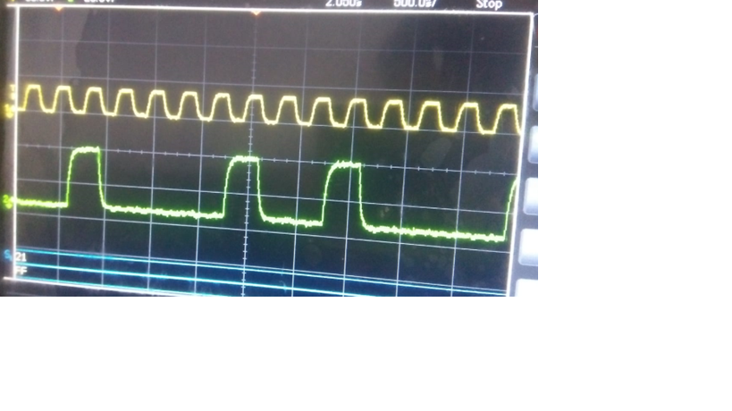
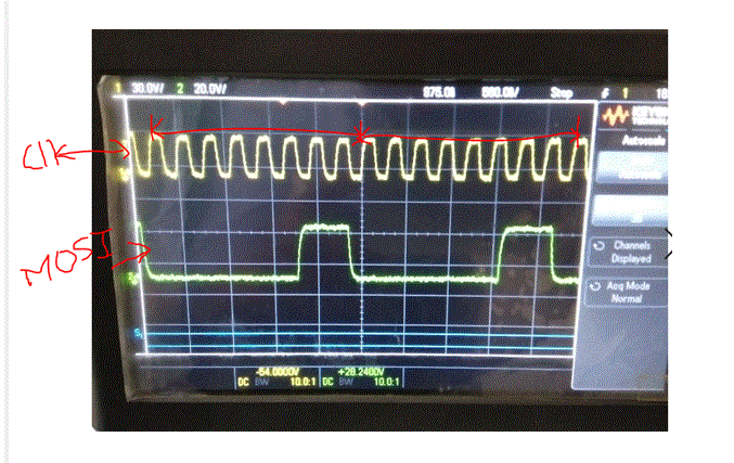
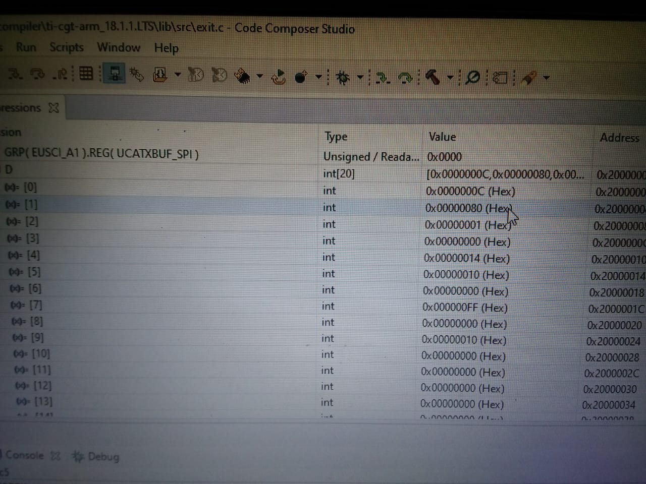
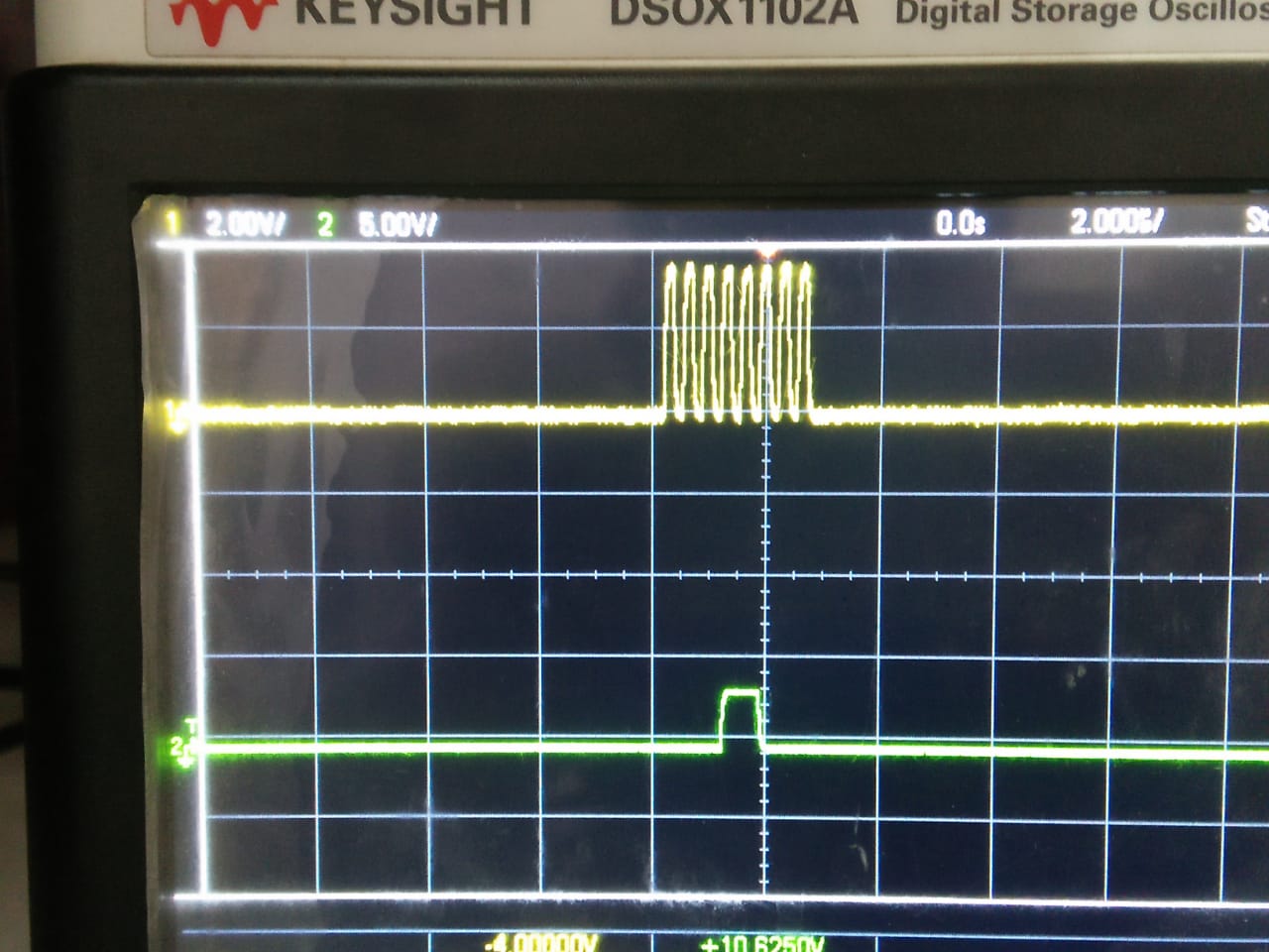
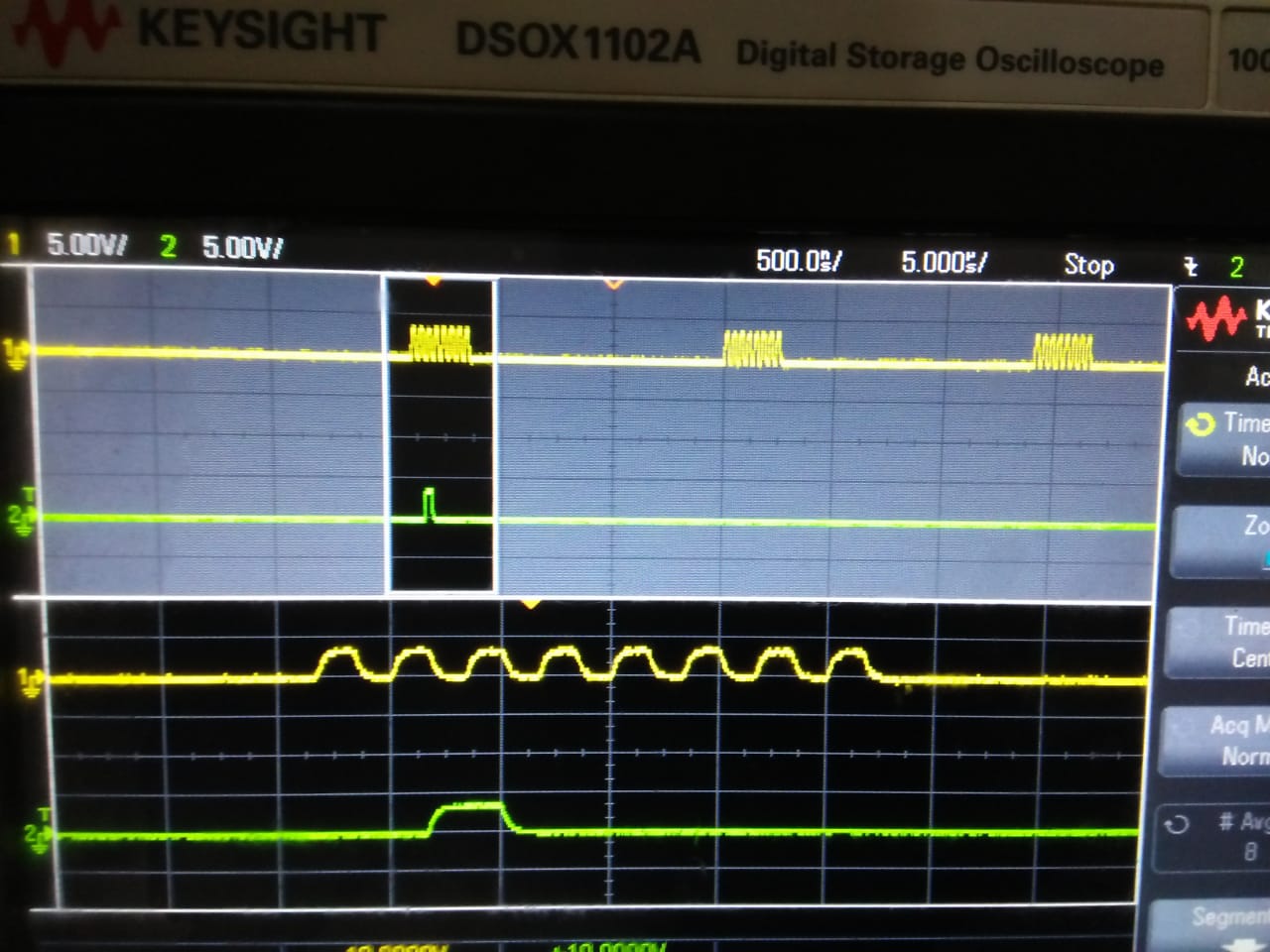
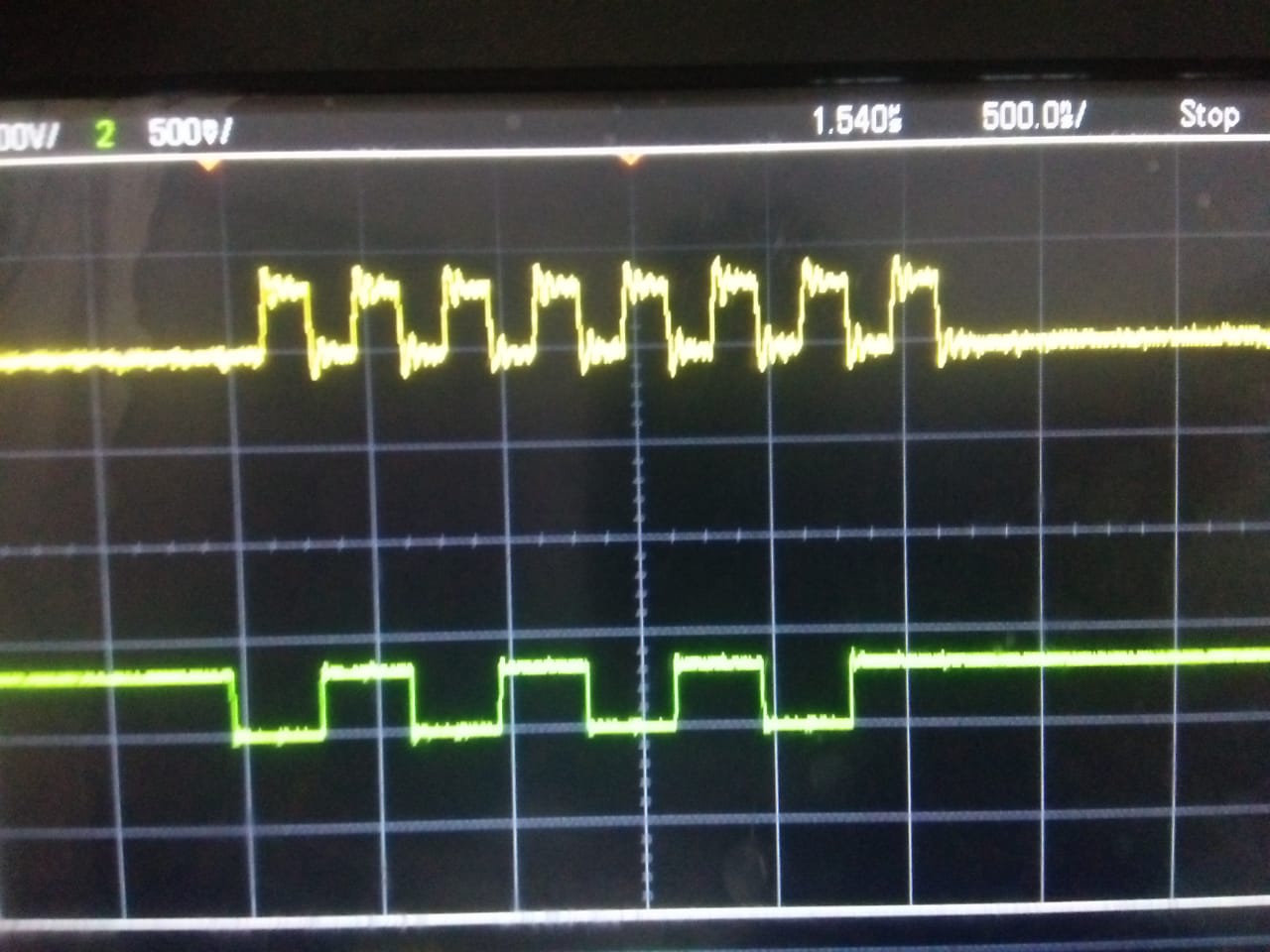
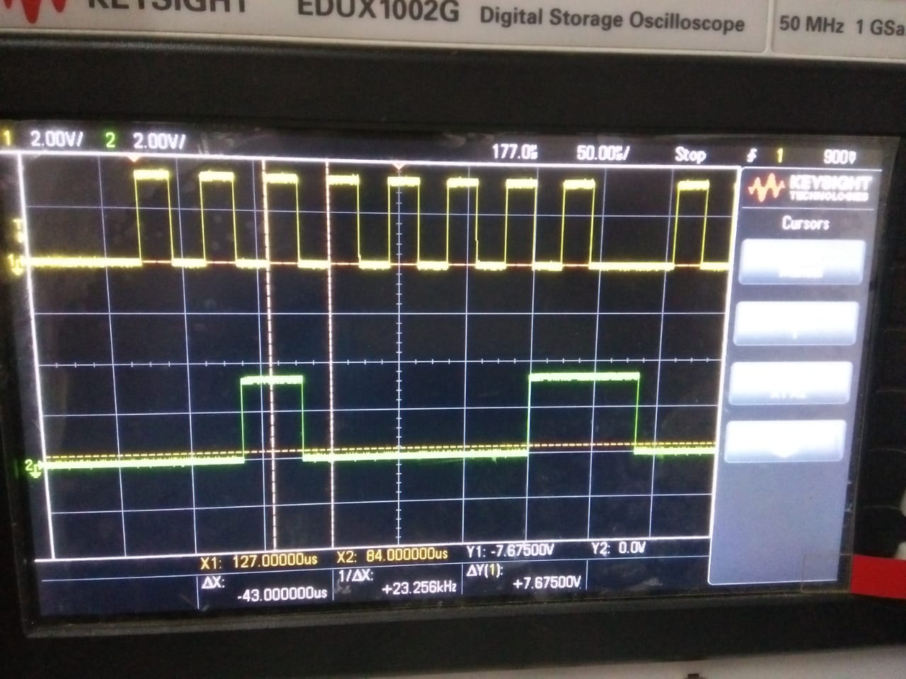
When the code is executed in a step by step manner the correct values are read about half the time but when the same code is executed in Run mode it gives 0x00 or 0xFF values.

#include "msp.h"
#include <ti/devices/msp432p4xx/driverlib/driverlib.h>
int i,D[16];
unsigned int D[16];
void dev_init_48M(void);
void SPI_INT();
void Read_Adc_reg();
void spi_tx(uint8_t txdata);
void  spi_rx();
void Reset();
void Delay_Ms();
void main(void)
{

WDT_A->CTL = WDT_A_CTL_PW | WDT_A_CTL_HOLD;   // stop watchdog timer
dev_init_48M();     //initialize device at 48MHz
P1->DIR &=~BIT5;
P1->REN |= BIT5;     //set p1.5 as input
P1->OUT |= BIT5;
P2->DIR |= BIT4;  // p2.4 as output cs pin to ADC
P1->DIR |= BIT4;  // p1.4 as output reset pin to ADC
P1->OUT |= BIT4;  // tie p1.4 to high
SPI_INT();        //spi setup
Read_Adc_reg();
}

void dev_init_48M(void)
{

/* Step 1: Transition to VCORE Level 1: AM0_LDO --> AM1_LDO */

while ((PCM->CTL1 & PCM_CTL1_PMR_BUSY));
PCM->CTL0 = PCM_CTL0_KEY_VAL | PCM_CTL0_AMR_1;
while ((PCM->CTL1 & PCM_CTL1_PMR_BUSY));


/* Step 2: Configure Flash wait-state to 1 for both banks 0 & 1 */
FLCTL->BANK0_RDCTL = (FLCTL->BANK0_RDCTL & ~(FLCTL_BANK0_RDCTL_WAIT_MASK)) |
FLCTL_BANK0_RDCTL_WAIT_1;
FLCTL->BANK1_RDCTL  = (FLCTL->BANK0_RDCTL & ~(FLCTL_BANK1_RDCTL_WAIT_MASK)) |
FLCTL_BANK1_RDCTL_WAIT_1;

/* Step 3: Configure DCO to 48MHz, ensure MCLK uses DCO as source*/
CS->KEY = CS_KEY_VAL ;                // Unlock CS module for register access
CS->CTL0 = 0;                           // Reset tuning parameters
CS->CTL0 = CS_CTL0_DCORSEL_5;           // Set DCO to 48MHz
// Select MCLK = DCO=48MHz and Configure SMCLK=MCLK/16= 3MHz(SMCLK source divider)
CS->CTL1 = CS->CTL1 & ~(CS_CTL1_SELM_MASK | CS_CTL1_DIVM_MASK) | CS_CTL1_SELM_3 | CS_CTL1_SELS_3 | CS_CTL1_DIVS_4;
CS->KEY = 0;             // Lock CS module from unintended accesses

// Enable global interrupt
__enable_irq();

}

void SPI_INT()
 {
    P2->SEL0 |= BIT1 | BIT2 | BIT3;                                           // set 4-SPI pin as second function

    //Configure microcontroller for SPI mode 1 (CPOL = 0, CPHA = 1)
    EUSCI_A1->CTLW0 |= EUSCI_A_CTLW0_SWRST;                                 // Put eUSCI state machine in reset
    EUSCI_A1->CTLW0 =  EUSCI_A_CTLW0_SWRST |                                  // Remain eUSCI state machine in reset
                       EUSCI_A_CTLW0_MST |                                        // Set as SPI master
                       EUSCI_A_CTLW0_CKPH |                                          // Clock phase select
                       EUSCI_A_CTLW0_SYNC |                                            // Set as synchronous mode
                       EUSCI_A_CTLW0_MSB|                                             // MSB first
                       EUSCI_A_CTLW0_MODE_0 |                                             // 3-pin mode
                       EUSCI_A_CTLW0_SSEL__SMCLK;                                    // SMCLK

    EUSCI_A1->BRW = 0x01;                                                    // /2,fBitCl0ock = fBRCLK/(UCBRx+1).
    EUSCI_A1->CTLW0 &= ~EUSCI_A_CTLW0_SWRST;                                // Initialize USCI state machine

 }

void Read_Adc_reg()
{

    Reset();
    spi_rx();

}
void Reset()
{
   Delay_Ms();
   spi_tx(0x06);
   Delay_Ms();
   Delay_Ms();

}
 void spi_tx(uint8_t txdata)
{

    P2->OUT &=~BIT4;            // CS at low
    Delay_Ms();
    while(!(EUSCI_A1->IFG & EUSCI_A_IFG_TXIFG));
    EUSCI_A1->TXBUF = txdata ;
    while( UCA1STATW & UCBUSY);
   P2->OUT |=BIT4;         // CS at high
  }
 void spi_txnop(uint8_t txdata)
 {


   while(!(EUSCI_A1->IFG & EUSCI_A_IFG_TXIFG));
    EUSCI_A1->TXBUF = txdata ;
   while( UCA1STATW & UCBUSY);

   }

 void  spi_rx()
 {
        spi_tx(0x22);        // RREG starting at 01h address(1st byte) status reg.
        spi_tx(0x10);        // 1 res. To read (2nd byte)
   P2->OUT &=~BIT4;            // CS at low
     for(i=0;i<16;i++)

  {

      spi_txnop(0x00);        //1 nop command to read one reg
      while (!(EUSCI_A1->IFG & EUSCI_A_IFG_RXIFG));
      D[i] = EUSCI_A1->RXBUF;   // Move data to a temporary buffer D
      Delay_Ms();
   }
 P2->OUT |=BIT4;             // CS at low
 }

 void Delay_Ms()
 {
   int k,j;
   for(k=0;k<100;k++)
  {
   for(j=0;j<2000;j++);
  }
 }

  • Hi Nikhil,

    Can you post a full schematic and your register settings as well? The image you sent is very small and the analog input connections are not shown.

    It would also be helpful to see the SPI communication lines using a logic analyzer, so we can look at what commands you are sending to the ADC and how it responds to those commands. This will help us determine if the ADC is being communicated with properly.

    -Bryan

  • Hi Brian

    I am attaching DSO screenshots and the controller and power schematic.

    After sending 0x06 21 00 00 command to read single register I get no output

  • Hi Brian

    I am attaching DSO screenshots and the controller and power schematic.

  • Here is the schematic from controller side, it is basically just direct connection between the MSP432 and the ADC. I tried with direct connection and with 47 ohm resistor in series. 

    After sending the single read register command in step by step manner I get following on the DSO

    0x06

    0x21

    followed by 0000.

    The expected response is 0x80 which is the default value of the status register but I get nothing

  • Hi Nikhil,

    Unfortunately none of your screenshots came through in your posts. Can you please re-post them? I usually save each image and attach it using the "Insert File" button.

    -Bryan

  • Hi Bryan

    Sorry about that. The website was glitchy last time. I am uploading the images again now.

  • Hi Nikhil,

    When I look at the image below, it seems like DIN is transitioning high-to-low/low-to-high when SCLK is transitioning high-to-low i.e SCLK falling edge. However, note that the ADC latches data on DIN on the SCLK falling edge, so if your digital signals are also transitioning during this time, the ADC might not get the command you intended.

    Can you confirm how you are triggering data on DIN (MOSI)?

    -Bryan

  • hi,

    now I am getting correct value of resistor when I reset the ADC using reset command here is My code for this

    ADS11s08 default resistor value reading working code


    #include "msp.h"
    #include <ti/devices/msp432p4xx/driverlib/driverlib.h>
    void delayMs(int n);
    int i,h,D[20];
    void main(void)
    {
        delayMs(100);
        P7->DIR |= BIT4;      // p2.4 as output cs pin to ADC
        P7->OUT &=~BIT4;      // cs held at low


        EUSCI_A1->CTLW0 = 0x0001;         /* disable UCA1 during config */
        /* clock phase/polarity:10, MSB first, 8-bit, master, 3-pin SPI, STE low active,
           synchronous mode, use SMCLK as clock source, STE for slave enable */
        EUSCI_A1->CTLW0 = 0x0A9C1;
        EUSCI_A1->BRW = 1;                /* 3 MHz / 1 = 3 MHz */
        EUSCI_A1->CTLW0 &= ~0x0001;       /* enable UCA1 after config */
        P2->SEL0 |= 0x0E;                            /* set alternate function to pinmap */
        P2->SEL1 &= ~0x0E;                       /* for P2.1, P2.2, P2.3 */
        while(!(EUSCI_A1->IFG & 2)) ;      //wait for transmit buffer empty
               EUSCI_A1->TXBUF = 0x06;          /* write the character */
                delayMs(1000);
    while(1)
    {
           for(i=0;i<17;i++)
           { 

                  while(!(EUSCI_A1->IFG & 2)) ; /* wait for transmit buffer empty */
                    EUSCI_A1->TXBUF = (0x20+i);          /* write the character */
                    while(EUSCI_A1->STATW & 1) ;      /* wait for transmit done */
                while(!(EUSCI_A1->IFG & 2)) ; /* wait for transmit buffer empty */
                     EUSCI_A1->TXBUF = 0x00;          /* write the character */
                     while(EUSCI_A1->STATW & 1) ;      /* wait for transmit done */
                while(!(EUSCI_A1->IFG & 2)) ; /* wait for transmit buffer empty */
                    EUSCI_A1->TXBUF = 0x00;          /* write the character */
                    while(EUSCI_A1->STATW & 1) ;      /* wait for transmit done */
                while (!(EUSCI_A1->IFG & EUSCI_A_IFG_RXIFG));
                    D[i] = EUSCI_A1->RXBUF;   // Move data to a temporary buffer D
                  h++;
                  delayMs(1000);}

    }
    }

    void delayMs(int n)
    {
        int k, j;
        for (j = 0; j < n; j++)
        for (k = 750; k > 0; k--);      /* delay */
    }

    now I get correct default value of Resistor and I take this value in D[17] array

    D[0]  - 0x0C

    D[0]  - 0x80

    D[0]  - 0x01

    D[0]  - 0x00

    D[0]  - 0x14

    D[0]  - 0x10

    D[0]  - 0x00

    D[0]  - 0xFF

    and so on, now I am tying to write this resistor with some value According to my requirement  but I am not get this value back when I am verifying that value using read command. I am getting  wrong value  for some resistor

    here is my new code for writing 0x55  to Reference Control Register (address = 05h)   and reading back this resistor to verify that resistor is correctly write or not

    #include "msp.h"
    #include <ti/devices/msp432p4xx/driverlib/driverlib.h>
    void delayMs(int n);
    int D;
    void main(void)
    {
        delayMs(100);
        P7->DIR |= BIT4;  // p2.4 as output cs pin to ADC
        P7->OUT &=~BIT4;  // cs held at low


        EUSCI_A1->CTLW0 = 0x0001;         /* disable UCA1 during config */
        /* clock phase/polarity:10, MSB first, 8-bit, master, 3-pin SPI, STE low active,
           synchronous mode, use SMCLK as clock source, STE for slave enable */
        EUSCI_A1->CTLW0 = 0x0A9C1;
        EUSCI_A1->BRW = 1;                /* 3 MHz / 1 = 3 MHz */
        EUSCI_A1->CTLW0 &= ~0x0001;       /* enable UCA1 after config */
        P2->SEL0 |= 0x0E;                            /* set alternate function to pinmap */
        P2->SEL1 &= ~0x0E;                       /* for P2.1, P2.2, P2.3 */
        while(!(EUSCI_A1->IFG & 2)) ;      //wait for transmit buffer empty
               EUSCI_A1->TXBUF = 0x06;          /* write the character */
                delayMs(1000);
    while(1)
    {

        // I am writing 0x55 value into Reference Control Register (address = 05h)


                  while(!(EUSCI_A1->IFG & 2)) ; /* wait for transmit buffer empty */
                        EUSCI_A1->TXBUF = 0x45 ;          /* write the character */
                        while(EUSCI_A1->STATW & 1) ;      /* wait for transmit done */
                        delayMs(100);
                    while(!(EUSCI_A1->IFG & 2)) ; /* wait for transmit buffer empty */
                         EUSCI_A1->TXBUF = 0x00;          /* write the character */
                         while(EUSCI_A1->STATW & 1) ;      /* wait for transmit done */
                         delayMs(100);
                    while(!(EUSCI_A1->IFG & 2)) ; /* wait for transmit buffer empty */
                        EUSCI_A1->TXBUF = 0x55;          /* write the character */
                        while(EUSCI_A1->STATW & 1) ;      /* wait for transmit done */
                   delayMs(1000);


          // I am reading Reference Control Register (address = 05h)

             while(!(EUSCI_A1->IFG & 2)) ; /* wait for transmit buffer empty */
                    EUSCI_A1->TXBUF = 0x25 ;          /* write the character */
                    while(EUSCI_A1->STATW & 1) ;      /* wait for transmit done */
                while(!(EUSCI_A1->IFG & 2)) ; /* wait for transmit buffer empty */
                     EUSCI_A1->TXBUF = 0x00;          /* write the character */
                     while(EUSCI_A1->STATW & 1) ;      /* wait for transmit done */
                while(!(EUSCI_A1->IFG & 2)) ; /* wait for transmit buffer empty */
                    EUSCI_A1->TXBUF = 0x00;          /* write the character */
                    while(EUSCI_A1->STATW & 1) ;      /* wait for transmit done */
                while (!(EUSCI_A1->IFG & EUSCI_A_IFG_RXIFG));
                    D = EUSCI_A1->RXBUF;   // Move data to a temporary buffer D
                  delayMs(1000);

    }
    }

    void delayMs(int n)
    {
        int k, j;
        for (j = 0; j < n; j++)
        for (k = 750; k > 0; k--);      /* delay */
    }

    here I am not getting 0x55 value back .please do needful and suggest what is wrong with my code

  • Hi Akshata,

    Can you check the DIN and DOUT signals on an oscilloscope or logic analyzer to see if you are transmitting and receiving the correct values from the ADC? This will help determine if the error is in the code or somewhere else.

    -Bryan

  • Hi,

    I am getting the same problem again to read the ADC resistor default value. below program I have written is working fine one day before but now I am not getting the default value of ADC resistor for the same program. I have to attach the DSO screen Shot here, ADC sends 60 mV noise signal back to the controller instead of  correct value.

    Here in Screenshot  -  Channel one is the Clock signal 

                                      -  Channel two is SOMI signal

    ADS11s08 default resistor value reading working code


    #include "msp.h"
    #include <ti/devices/msp432p4xx/driverlib/driverlib.h>
    void delayMs(int n);
    int i,h,D[20];
    void main(void)
    {
        delayMs(100);
        P7->DIR |= BIT4;      // p2.4 as output cs pin to ADC
        P7->OUT &=~BIT4;      // cs held at low


        EUSCI_A1->CTLW0 = 0x0001;         /* disable UCA1 during config */
        /* clock phase/polarity:10, MSB first, 8-bit, master, 3-pin SPI, STE low active,
           synchronous mode, use SMCLK as clock source, STE for slave enable */
        EUSCI_A1->CTLW0 = 0x0A9C1;
        EUSCI_A1->BRW = 1;                /* 3 MHz / 1 = 3 MHz */
        EUSCI_A1->CTLW0 &= ~0x0001;       /* enable UCA1 after config */
        P2->SEL0 |= 0x0E;                            /* set alternate function to pinmap */
        P2->SEL1 &= ~0x0E;                       /* for P2.1, P2.2, P2.3 */
        while(!(EUSCI_A1->IFG & 2)) ;      //wait for transmit buffer empty
               EUSCI_A1->TXBUF = 0x06;          /* write the character */
                delayMs(1000);
    while(1)
    {
           for(i=0;i<17;i++)
           { 

                  while(!(EUSCI_A1->IFG & 2)) ; /* wait for transmit buffer empty */
                    EUSCI_A1->TXBUF = (0x20+i);          /* write the character */
                    while(EUSCI_A1->STATW & 1) ;      /* wait for transmit done */
                while(!(EUSCI_A1->IFG & 2)) ; /* wait for transmit buffer empty */
                     EUSCI_A1->TXBUF = 0x00;          /* write the character */
                     while(EUSCI_A1->STATW & 1) ;      /* wait for transmit done */
                while(!(EUSCI_A1->IFG & 2)) ; /* wait for transmit buffer empty */
                    EUSCI_A1->TXBUF = 0x00;          /* write the character */
                    while(EUSCI_A1->STATW & 1) ;      /* wait for transmit done */
                while (!(EUSCI_A1->IFG & EUSCI_A_IFG_RXIFG));
                    D[i] = EUSCI_A1->RXBUF;   // Move data to a temporary buffer D
                  h++;
                  delayMs(1000);}

    }
    }

    void delayMs(int n)
    {
        int k, j;
        for (j = 0; j < n; j++)
        for (k = 750; k > 0; k--);      /* delay */
    }

    above code work fine one day before but now it is not working, I didn't understand where is a problem is in code or hardware please suggest any solution.

    Is ADC working fine or not?  How to check ADC is working or not ?

  • Hi Akshata,

    I see from the initial schematic that Nikhil posted that you have two different ground symbols for AVSS and DGND. This implies a split ground plane, which we generally do not recommend. If there are ground potential differences between the analog and digital grounds this could certainly cause communication issues.

    Either way, your digital communication signals are noisy, which usually indicates a grounding or layout issue. In other words, I am not so sure this is a code issue at this point, given the information you have already provided. Here are some general tips about this topic: https://e2e.ti.com/support/data-converters/f/73/t/755516

    -Bryan

  • Hi,

    I try to find a noise source in my system and it is noticed that our DC power supply emit noise in my system, so I used another power supply for testing and it seem that there is a very clear signals waveform without much noise on the signal and now sometimes I get the correct default value of ADC resistor but not every time.

    If I try multiple times to read the default value of the ADC resistor then I get a correct result sometimes. once I get the correct default value of the ADC resistor it giving me the same result until the system is ON and when I switch off the system and again start the system then it not giving me the correct default value of the ADC resistor.

    so I don't understand where is the issue is in software code or in hardware, if the software code is not fine then ADC should not be responded back but sometimes it gives the correct result. 

    here CCS screenshot for the correct default value of ADC resistor

    DSO screenshot when ADC giving the correct result -

    Channel 1- Clock

    Channel 2 - SOMI   - here is very clear waveform is getting 

    here is a  DSO screenshot with ZOOM picture

    when ADC not giving me a result then at SOMI signal we get nothing and at the same time whatever command sent by the microcontroller to ADC for reading ADC resistor is correctly sent to ADC hence we don't

    where is the problem occur?

    One thing I noticed when I verifying that the microcontroller is sending the correct data  to  ADC or not, I was trying to send 0x55 to ADC over the SOMI line then the idle state of the SOMI line is high

    this waveform is capture at the time when the noisy power supply is used

    Channel 1 - Clock

    Channel 2 - SOMI  ( I am sending 0x55 over SOMI to ADC )

    and when I remove this supply I used another power supply then the same SPI  setting idle sate of SOMI is  LOW

    Channel 1- clock

    Channel 2 - SOMI (here again I am sending 0x55 over SOMI to ADC)


    How this difference is coming for the same SPI setting?

    Please suggest what is wrong and provide a solution for these.

  • Hi Akshata,

    Can you probe DIN on the scope as well to see what signal you are sending to the ADC? I would also suggest trying to read back one register for now, just to keep it simple. Power up the device, send the RREG command for one register and see what the output is while probing DIN, DOUT, SCLK and CS. If you have a logic analyzer that would help as well

    You should also ensure that the device is being powered properly and the the voltages are maintained throughout the conversion process i.e. no voltage droop that could cause a POR condition.

    Note that the split ground plane on your PCB could still be an issue here.

    -Bryan

  • Hi,

    as your suggestion I tried to read single register and observed that clock and DIN is not synchronize as per datasheet of ADS114s08 and I am using  SPI mode one as per datasheet of ADC

    here I am reading status resistor of ADC for am sending RREG command (3 byte Command)

    1st byte    - 0x21 

    channel 1 - clock

    channel 2 - MOSI

    here am sending 0x21( 1st byte of command ) binary equivalent is - 0010 0001

     as per datasheet data change occur at raising edge and data latch at falling edge but here data change at falling edge and latch at raising edge but SPI setting is OK as per ADC datasheet    what is reason behind these please suggest the solution to overcome this issue?


    code for above task -

    #include "msp.h"
    #include <ti/devices/msp432p4xx/driverlib/driverlib.h>
    void delayMs(int n);
    int i,h,D;
    void main(void)
    { WDT_A->CTL = WDT_A_CTL_PW | WDT_A_CTL_HOLD;       // stop watchdog timer
    while ((PCM->CTL1 & PCM_CTL1_PMR_BUSY));
          PCM->CTL0 = PCM_CTL0_KEY_VAL | PCM_CTL0_AMR_1;
          while ((PCM->CTL1 & PCM_CTL1_PMR_BUSY));


         /* Step 2: Configure Flash wait-state to 1 for both banks 0 & 1 */
          FLCTL->BANK0_RDCTL = (FLCTL->BANK0_RDCTL & ~(FLCTL_BANK0_RDCTL_WAIT_MASK)) |
                  FLCTL_BANK0_RDCTL_WAIT_1;
          FLCTL->BANK1_RDCTL  = (FLCTL->BANK0_RDCTL & ~(FLCTL_BANK1_RDCTL_WAIT_MASK)) |
                  FLCTL_BANK1_RDCTL_WAIT_1;

          /* Step 3: Configure DCO to 48MHz, ensure MCLK uses DCO as source*/
          CS->KEY = CS_KEY_VAL ;                  // Unlock CS module for register access
          CS->CTL0 = 0;                           // Reset tuning parameters
          CS->CTL0 = CS_CTL0_DCORSEL_1;           // Set DCO to 48MHz
          // Select MCLK = DCO=48MHz and Configure SMCLK=MCLK/16= 3MHz(SMCLK source divider)
          CS->CTL1 = CS->CTL1 & ~(CS_CTL1_SELM_MASK | CS_CTL1_DIVM_MASK) | CS_CTL1_SELM_3 | CS_CTL1_SELS_3 | CS_CTL1_DIVS_7;
          CS->KEY = 0;                            // Lock CS module from unintended accesses

          // Enable global interrupt
          __enable_irq();
        P7->DIR |= BIT4;  // p2.4 as output cs pin to ADC
        P7->OUT &=~BIT4;  // cs held at low
        EUSCI_A1->CTLW0 |= EUSCI_A_CTLW0_SWRST;          // Put eUSCI state machine in reset
           EUSCI_A1->CTLW0 = EUSCI_A_CTLW0_SWRST |          // Remain eUSCI state machine in reset
                             EUSCI_A_CTLW0_MST |            // Set as SPI master
                             EUSCI_A_CTLW0_CKPH |           // Clock phase select
                             EUSCI_A_CTLW0_SYNC |           // Set as synchronous mode
                             EUSCI_A_CTLW0_MSB|             // MSB first
                             EUSCI_A_CTLW0_MODE_0 |         // 3-pin mode
                             EUSCI_A_CTLW0_SSEL__SMCLK;     // SMCLK

           EUSCI_A1->BRW = 0x01;                            // /2,fBitCl0ock = fBRCLK/(UCBRx+1).
           EUSCI_A1->CTLW0 &= ~EUSCI_B_CTLW0_SWRST;         // Initialize USCI state machine
        P2->SEL0 |= 0x0E;                            /* set alternate function to pinmap */
        P2->SEL1 &= ~0x0E;                       /* for P2.1, P2.2, P2.3 */
        while(!(EUSCI_A1->IFG & 2)) ;      //wait for transmit buffer empty
               EUSCI_A1->TXBUF = 0x06;          /* write the character */
                delayMs(1000);
      while(1)
      {
               while(!(EUSCI_A1->IFG & 2)) ; /* wait for transmit buffer empty */
                    EUSCI_A1->TXBUF = (0x21);          /* write the character */
                   while(EUSCI_A1->STATW & 1) ;      /* wait for transmit done */

                while(!(EUSCI_A1->IFG & 2)) ; /* wait for transmit buffer empty */
                     EUSCI_A1->TXBUF = 0x00;          /* write the character */
                    while(EUSCI_A1->STATW & 1) ;      /* wait for transmit done */

                while(!(EUSCI_A1->IFG & 2)) ; /* wait for transmit buffer empty */
                    EUSCI_A1->TXBUF = 0x00;          /* write the character */
                    while(EUSCI_A1->STATW & 1) ;      /* wait for transmit done */
                while (!(EUSCI_A1->IFG & EUSCI_A_IFG_RXIFG));
                    D = EUSCI_A1->RXBUF;   // Move data to a temporary buffer D
                  h++;
                  delayMs(1000);

    }
    }

    void delayMs(int n)
    {
        int k, j;
        for (j = 0; j < n; j++)
        for (k = 750; k > 0; k--);      /* delay */
    }

  • Hi Akshata,

    Would it be possible to double check the digital interface settings again? You are correct that the ADC latches data on the SCLK falling edge, so if you are showing SCLK and DIN in your scope shots then your command (0x21h) is not being read properly by the ADC.

    -Bryan

  • Hi, 

    SPI setting is correct as per the datasheet

    SPI interface of the microcontroller to SPI mode 1 (CPOL = 0, CPHA =1);

    CS/ - Set low;

    and I want to know that what should be clock frequency of spi ? I tried for 3MHz 

    I am using internal DSO in the project as the clock source, 

    if anything wrong with my spi setting or schematic then, please suggest the best solution for this?

    thank you.

  • Hi Akshata,

    Please note that not all MCU datasheets use the same terminology to mean the same thing. In this case, the MSP432P manual uses UCCKPH (phase) and UCCKPL (polarity).

    In the MCU datasheet, table 25-3 says

    • if UCCKPH = 0, then data is changed on the first UCLK edge and captured on the following edge.
    • If UCCKPL = 0, then the clock polarity is low when inactive

    Taken together, the "first UCLK edge" if UCLK idles low is a low to high transition, and the "following edge" is high to low transition. These are the settings you want, since you want to capture data on DIN on the UCLK (SCLK) falling edge, according to section 9.5.1.3 in the ADS114S08 datasheet. Please make sure your settings are correct in your code.

    -Bryan

  • Hi,

    I change setting as you suggest and I got the correct value of Resistor and I am able to write and read resistor configuration.

    Thank you.

  • Hi Akshata,

    Good to know, I am glad this is resolved. If you have a new query, please start a new thread and we will respond to your question there.

    -Bryan

  • Q. How to convert ADS114s08  ADC output code into equivalent RTD  Temprature?

  • Hi,

    Now I get  the ADC output code and I want to convert this code into equivalent temperature. how I perform this calculation.

    at room temp. I get   0x1C00 code and I want to convert this code into Temp. I use ADS calculator it show me the output voltage of RTD  which 109mV

    Please provide answer with good example?

  • HI Akshata,

    I would recommend checking out our temperature sensor firmware for the ADS1x4S0x devices: https://www.ti.com/tool/ADC-TEMP-SENSOR-FW

    This includes the look-up tables and equations required to convert the ADC's output code to a temperature given the specific RTD you are using.

    -Bryan