This thread has been locked.

If you have a related question, please click the "Ask a related question" button in the top right corner. The newly created question will be automatically linked to this question.

ADS1248: No excitation current output from IEXC1

Part Number: ADS1248


Hi there,

We are using the ADS1248 in our new design and the readings of the line ANI_TAT_HI_ELP (upper left corner of the below schematic)) fluctuate greatly without a clear pattern within the full binary range, and it is always changing so we cannot interpret. Its implementation is shown in the following figure:

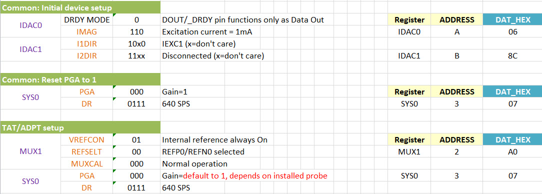
We believe that we're performing the correct configuration in its registers by SW, with excitation current=1mA (IMAG=110b), using IEXC1 (I1DIR=1000), selecting the REFP0/REFP1 couple as reference input. However during runtime, the voltage measured over the resistor R31 that is fed by IEXC1 is always 0, which indicates that no current was output from pin #20 of the ADS1248.

For trials, we've already turned the internal reference to always ON (VREFCON=1) or OFF, and we've even removed both diodes (D5 and D6) from the circuit, and the results remain the same (fluctuating).

Anything that we might have left out in its configuration or error in our circuit design?

Thank you for any help.

  • I just want to add that this channel is an interface to a 3-wire RTD-type probe (Total Air Temperature probe), and that all other channels not needing the excitation current were correctly acquired by the A/D.

  • Update: We've confirmed that the excitation current is missing from IEXC1 (0.00 A), and below is the configuration to the ADS1248 to output the excitation current on pin IEXC1, just in case one may see something wrong here:

  • Hi Chuck,

    What type of RTD are they using, a Pt100, Pt1000, etc.?

    Why are caps C40 and C44 included in this schematic? I would have thought the filter caps (C39, C41, C42) would be sufficient, but maybe they serve another purpose?

    Can you also explain what is meant by the "results are fluctuating"? Is the voltage across the RTD fluctuating, or are they measuring the IDAC current somewhere (e.g. across R31) and that is fluctuating? What are the results fluctuating between? Can you post some data to review?

    There is nothing obviously wrong with the circuit you have provided, so I will need some more details. Thanks!

    -Bryan

  • Hello Bryan,

    Sorry for the delay in responding to your questions. 

    It has turned out that the excitation current programming by the SW didn't get through to the corresponding register, which explains my problems. Therefore answering to your questions above might not be relevant in this case, instead I would like to explain and to see if you could help.

    Yeah, after taking the same steps in programming the excitation current at the beginning or end of the SW loop control/reading cycles (rather than during initialization), everything looks good, and we've obtained the right level of voltage in every channels (6 in each of the two connected ADS1248). However, I don't know why the steps in achieving such during initialization didn't work out. Below is my initialization sequences, at approximately 1.5s after power-up, so everything should be stable:

    TG0 Register BUFID Chip-Select MibSPI_TXRAM
    SDATAC - 0 nCS[1&5] 0x881D0016
    WREG SYS0 1 nCS[1&5] 0x981D0043
    WREG 0 2 nCS[1&5] 0x981D0000
    Data SYS0 3 nCS[1&5] 0x881D0007
    WREG IDAC0 4 nCS[1&5] 0x981D004A
    WREG 1 5 nCS[1&5] 0x981D0001
    Data IDAC0 6 nCS[1&5] 0x981D0006
    Data IDAC1 7 nCS[1&5] 0x881D008C
    SYNC - 8 nCS[1&5] 0x981D0004
    SYNC - 9 nCS[1&5] 0x881D0004
    SELFOCAL OFC1,2 10 nCS[1&5] 0x841D0062
    TG1
    RREG MUX0 11 nCS[1] 0x983D0020
    RREG 15 12 nCS[1] 0x983D000F
    NOP MUX0 13 nCS[1] 0x983D00FF
    NOP VBIAS 14 nCS[1] 0x983D00FF
    NOP MUX1 15 nCS[1] 0x983D00FF
    NOP SYS0 16 nCS[1] 0x983D00FF
    NOP OFC0 17 nCS[1] 0x983D00FF
    NOP OFC1 18 nCS[1] 0x983D00FF
    NOP OFC2 19 nCS[1] 0x983D00FF
    NOP FSC0 20 nCS[1] 0x983D00FF
    NOP FSC1 21 nCS[1] 0x983D00FF
    NOP FSC2 22 nCS[1] 0x983D00FF
    NOP IDAC0 23 nCS[1] 0x983D00FF
    NOP IDAC1 24 nCS[1] 0x983D00FF
    NOP GPIOCFG 25 nCS[1] 0x983D00FF
    NOP GPIODIR 26 nCS[1] 0x983D00FF
    NOP GPIODAT 27 nCS[1] 0x843D00FF

    I've made sure that the START signal is and remains active before sending out TG0 (MibSPI), and there is a delay of 50ms between TG0 and TG1, following the SELFOCAL command, which should take 26ms to complete (with a SPS=640).

    I understand that if the SPS=640 wasn't taken, the SELFOCAL would take more than 2s to complete. To make sure, I've also removed the SELFOCAL command but the results is still the same: registers readback (TG1) did not contain the programmed values, as shown in the MIBSPI3_RXRAM_BASE capture below:

    Do you see anything wrong with my steps?

    Many thanks.

  • Hi Chuck,

    Glad you solve the initial problem.

    Can you try to read back the IDAC registers immediately after writing them? So, before the 2x SYNC commands? Let's just make sure the device acknowledges these WREGs

    And you are holding START high during this process correct? You said "active", but I just wanted to confirm.

    You also said you are able to get this to work at the beginning or end of a SW loop, but not at initialization. Is there anything you are doing differently in that loop?

    -Bryan

  • Reading immediately following write to IDAC0 and IDAC1 does work correctly:

    MIBSPI3_RXRAM[10] = IDAC0 = 0x96

    MIBSPI3_RXRAM[11] = IDAC1 = 0x8C

    But again, not with TG1.

    So I replaced SYNC, SYNC, SELFOCAL by NOP, still the same issue, same readback values with TG1, which are:

    MIBSPI3_RXRAM[27] = IDAC0 = 0x90

    MIBSPI3_RXRAM[28] = IDAC1 = 0xFF

    This is saying that IDAC0 and IDAC1 did not keep their values when TG0 ends, even when only NOP were executed, or after TG1, 

    And yes, the signal START is active high, so when I say it is active, it is indeed high during the whole process (TG0+TG1).

    Nothing is different in the SW loop, I've just copied the 4 instructions from it and pasted it into the initialization part shown above, one exception is that it is doing that every cycle.

  • Hi Chuck,

    So we've determined that the device does read the registers correctly, so that is good.

    Can you explain what is happening between issuing the commands in TG0 and TG1? Is that just a 50ms delay? Are there any other commands being issued or traffic on the SPI lines during this time? Is there a chance that the RESET pin is being toggled?

    If you remove the 2x SYNC commands, the SELFOCAL command, and the corresponding delay, then TG0 followed by TG1 should be no different than the experiment you just did where you issues the RREG commands immediately after setting the IDACs. The only difference I can see is that the RREG command in TG1 is reading back all registers while the RREG command in TG0 is only reading back two.

    -Bryan

  • Hi Bryan,

    The MibSPI3 is solely used for the ADS1248, and between TG0 and TG1 the only thing is the 50ms delay. I’ll check the reset pin signal tomorrow.

    I do agree with your statement of the last paragraph.

    Cheers!

  • Thanks Chuck, let us know. If you have a logic analyzer you can look at all of the communication lines to see if there is anything out of the ordinary between commands. Please post any scope shots you take for reference.

    FYI, responses may delayed over the next few days due to the holiday.

    -Bryan

  • Hello Bryan,

    You're totally right. It turned out that the reset logic has issued a signal to reset the ADS1248 after its configuration, therefore the observed results.

    Thank you very much for your suggestion and support.

    Regards.

  • Thanks Chuck, glad you got it figured out.

    -Bryan