This thread has been locked.

If you have a related question, please click the "Ask a related question" button in the top right corner. The newly created question will be automatically linked to this question.

ADS1235: Schematic Review

Part Number: ADS1235
Other Parts Discussed in Thread: UCC27524

Hi everyone.

As I've posted on another thread, we are developing an equipment for process control with a load cell. We need to read values and perform calculations in less than 1ms.

We have developed this circuit that I'm posting here for your kindly review.

Starting with the power management. We will have only one of power source from a 24VDC PSU. So we are using a Synchronous Step-down Voltage Converter(LMR33620ADDA), which seems to be very efficient and has low EMI and low switching noise. Before that we have two LDO, one for AVDD(5V) and other for DVDD(3.3v) which we'll use to supply the MCU and digital supply for ADC1235

Here we are representing the  load cell connections

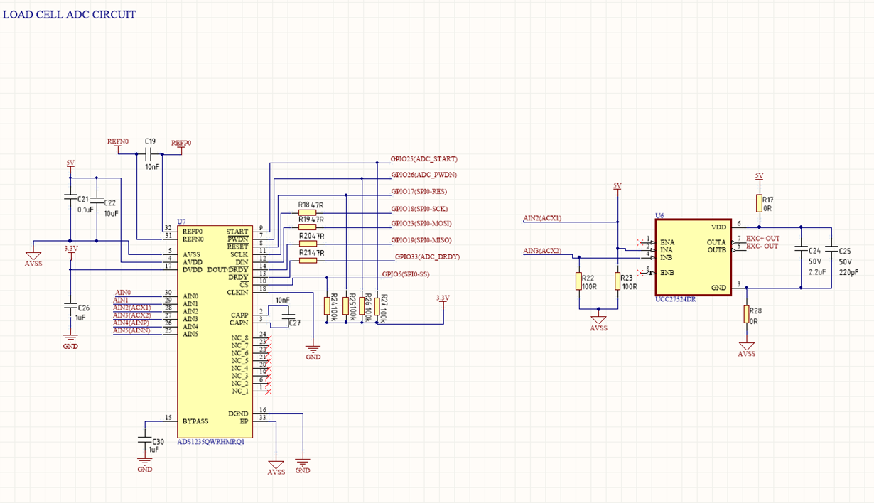
And here we represent the ADC circuit with ADS1235 and UCC27524 for switching the AC Excitation

I would be grateful for any help you are able to provide

  • Hi Guilherme,

    The only issue that stands out to me are the connections to U6.  You don't want to tie INA high if you intend to control the excitation direction as there will be contention from the driving GPIO when tied directly to +5V.

    Best regards,

    Bob B

  • Hi Mr Benjamin,

    Thanks for you answer. That was a mistake of mine. Take a look at the correction:

    I have a few doubts:

    1)AIN0 and AIN1 are not being used. They may be left floating, or need to be pulled up?

    2)I have read the ADS1235 Datasheet, but just to confirm, the 300mA (max provided by LDO) is enough for this application, right?

    3) I chose to control the ADS1235 START, PWND and RESET by the MCU. Is that a good practice? Or is better to keep them in DVDD, GND, GND respectively?

    Thank you

  • Hi Guilherme,

    Be careful not to assume that you will get higher levels of performance using ac excitation compared to dc.  I would compare the results using both methods.  Something that is often not considered is the settling time and the length of total conversion time when using ac excitation.  With dc excitation it is possible to run at slower data rates which will also offer lower noise.  The ac excitation will need to run much faster to get the same overall throughput with increased noise. Which method you wish to use depends on what issue you are trying to solve.  If offset is the issue, then maybe just using chop mode with dc excitation would be a better choice.  I have seen results in process control systems where ac excitation was used but the results were much worse than dc excitation.  For example, any vibrations during ac excitation can affect the conversion result as the effect of the excitation and the vibration on the load cell can appear as additional noise while the load cell is settling. 

    Regarding the schematic, you could directly tie U6 VDD directly to AVDD and similar for connecting GND to AVSS.  These were option resistors used on the EVM that you should not need.  Removing the resistors (R17 and R28) will lower the inductance and albeit small resistance in the path.  For sure I would remove R28 and tie GND directly to AVSS.

    I would also recommend a single ground plane where AVSS and GND are connected together to the same plane.

    Below are my additional responses to your questions.

    1)AIN0 and AIN1 are not being used. They may be left floating, or need to be pulled up? [Bob]  There is a section on unused inputs in section 9.1.3 of the ADS1235 datasheet.  I would suggest that instead of directly connecting the inputs to AVDD use a pullup resistor.  The reason being is that you will need to configure the ADS1235 to 4-wire ac excitation even though you are only using 2 of the GPIO for control.  If you were to inadvertently have the unused GPIO switched to output mode, the current could be excessive through the pin if the GPIO was set low.  Using a pullup to current limit would be a safer approach.

    2)I have read the ADS1235 Datasheet, but just to confirm, the 300mA (max provided by LDO) is enough for this application, right? [Bob] I don't know the entire circuit or the load cell resistance you are using for the 5V, but 300mA should be sufficient in a normal application.  Most likely the greater current draw will be from the excitation of the bridge as compared to the ADS1235.

    3) I chose to control the ADS1235 START, PWND and RESET by the MCU. Is that a good practice? Or is better to keep them in DVDD, GND, GND respectively? [Bob] Setting the pin states to a fixed value depends on whether or not you intend to use the intended purpose of the pins.  For example, if you never intend to use the PWDN pin, then you can tie it high instead of controlling through the micro.  The same for START.  I would recommend that you control the RESET pin.  If for some reason the ADS1235 would get into an odd operating state, you can always reset the device if you have control of that pin.

    Best regards,

    Bob B

  • Hi Mr. Benjamin.
    For my application, vibration will be a big issue, because this equipment is meant to be used on a high speed rotating filling machine, for measuring the bottle weight and stop the filling process with high precision (less than 1g). From where i have studied, the ADS1235 would be the best option for this application. Am I Right?
    So i did the changes you suggested. This is how its now:

    Chossing a 4 layers PCB (because my manufacurer doesn't makes it with 3 layers). If we use top and bottom for circuit traces, would be better using the 2 inner layers for GND and AVSS or one for GND/AVSS and other for +5V?

    Thanks

  • Hi Guilherme,

    The ADS1235 would be the appropriate device for your design.  The circuit changes look good to me.  For a 4-layer board I would suggest routed power with signal/power on the outer layers and both inner layers as ground.  AVSS and GND should be the same potential (do not split the ground).  When routing signals, just make sure that the digital signals do not cross into the analog domain.

    Best regards,

    Bob B

  • Ok. Thanks a lot for your support!

  • Hi Mr Benjamin,


    We are starting the PCB Layout and another issue has come about this project and I'd like your opinion.
    We have the option to build one PCB with all the circuits (power supply management, MCU, ADC circuit, 24VDC output for valves driving), or make separated PCBs with a back plane for data bus and power supply. The idea of this second option has come because I think that a separated PCB for ADC circuit could be more immune to other circuits noise. Does it make sense? Maybe one PCB for Supply management+MCU+Output Driving, and other just for ADC connected through a backplane for SPI + Power Supply?

    Thank you

  • Hi Guilherme,

    There is good and bad about both approaches.  There can be proximity issues with large transient currents.  However, adding cabling/interconnect between two boards has its own set of issues.  It is difficult for me to speculate on which method would be the best approach as I know little about your system.  In making these types of decisions you should list the benefits of both methods and determine the best course of action.

    Best regards,

    Bob B