This thread has been locked.

If you have a related question, please click the "Ask a related question" button in the top right corner. The newly created question will be automatically linked to this question.

DAC7760: SPI Read Issue

Part Number: DAC7760

Hi Ti,

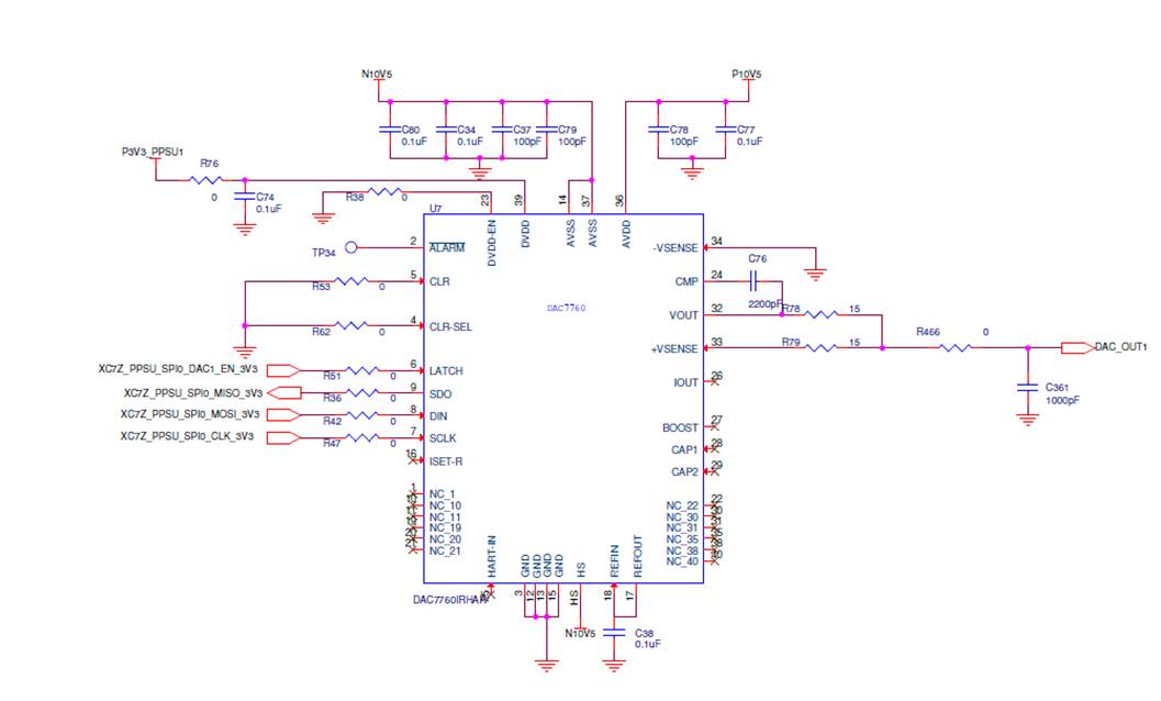
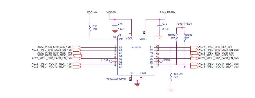
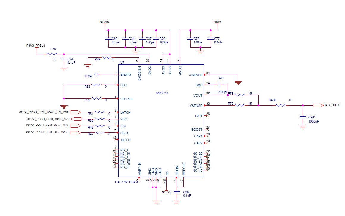
We are using two DAC7760 to capture range of voltages
1. ±5 V (dac7760_circuit attached)


2. 0V to 10V

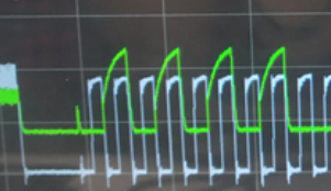
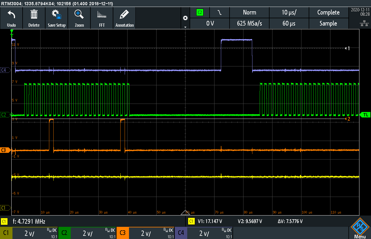
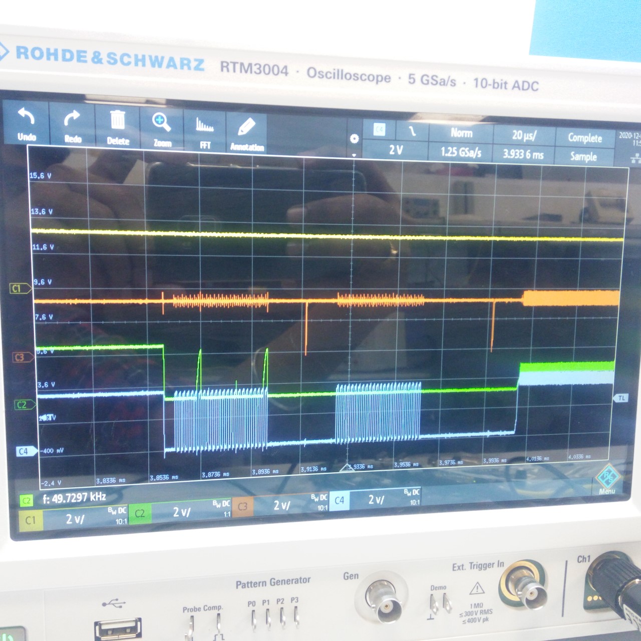
Read dac register form both DAC7760 is not working, SPI read/write timing is matching with datasheet(please refer the attached).

Following are the 24 bit spi write in init sequence
1. 56 0001(init1.jpeg)

2. 01 0001 (init2.png)

3. 55 1002 (init3.png)


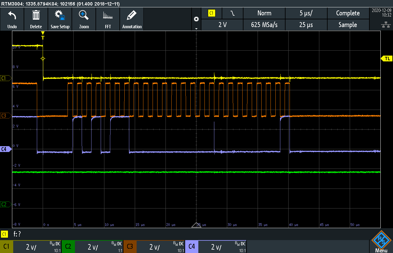
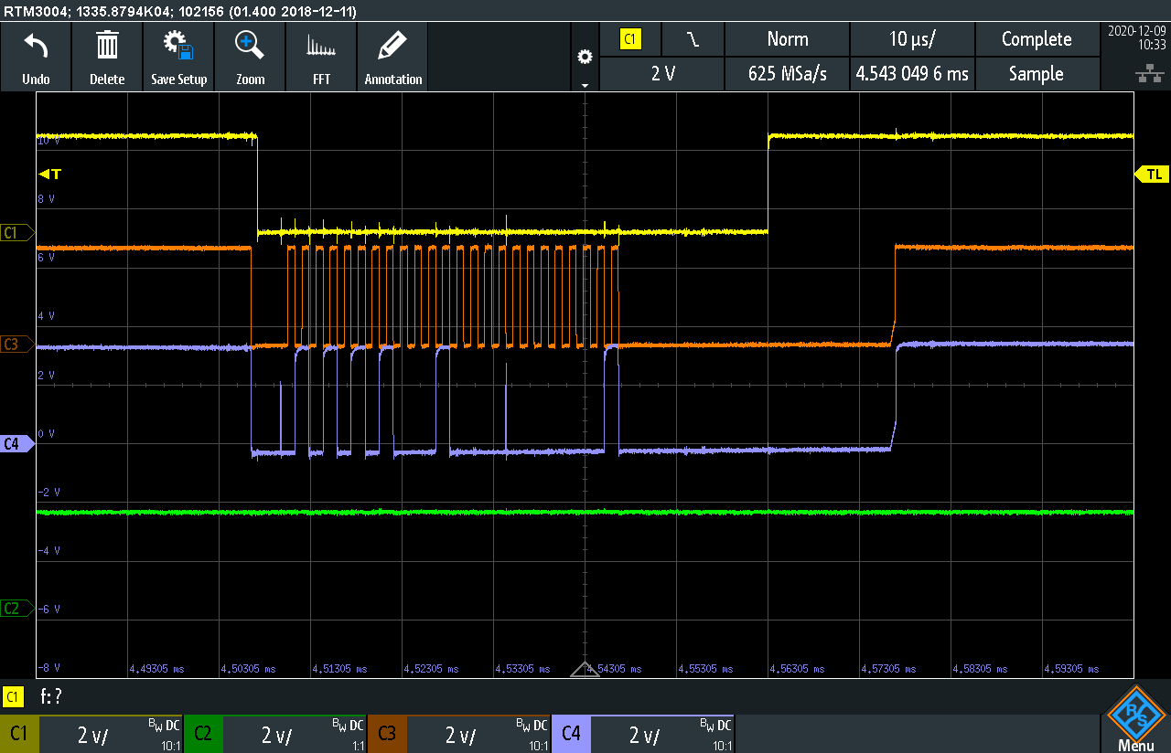
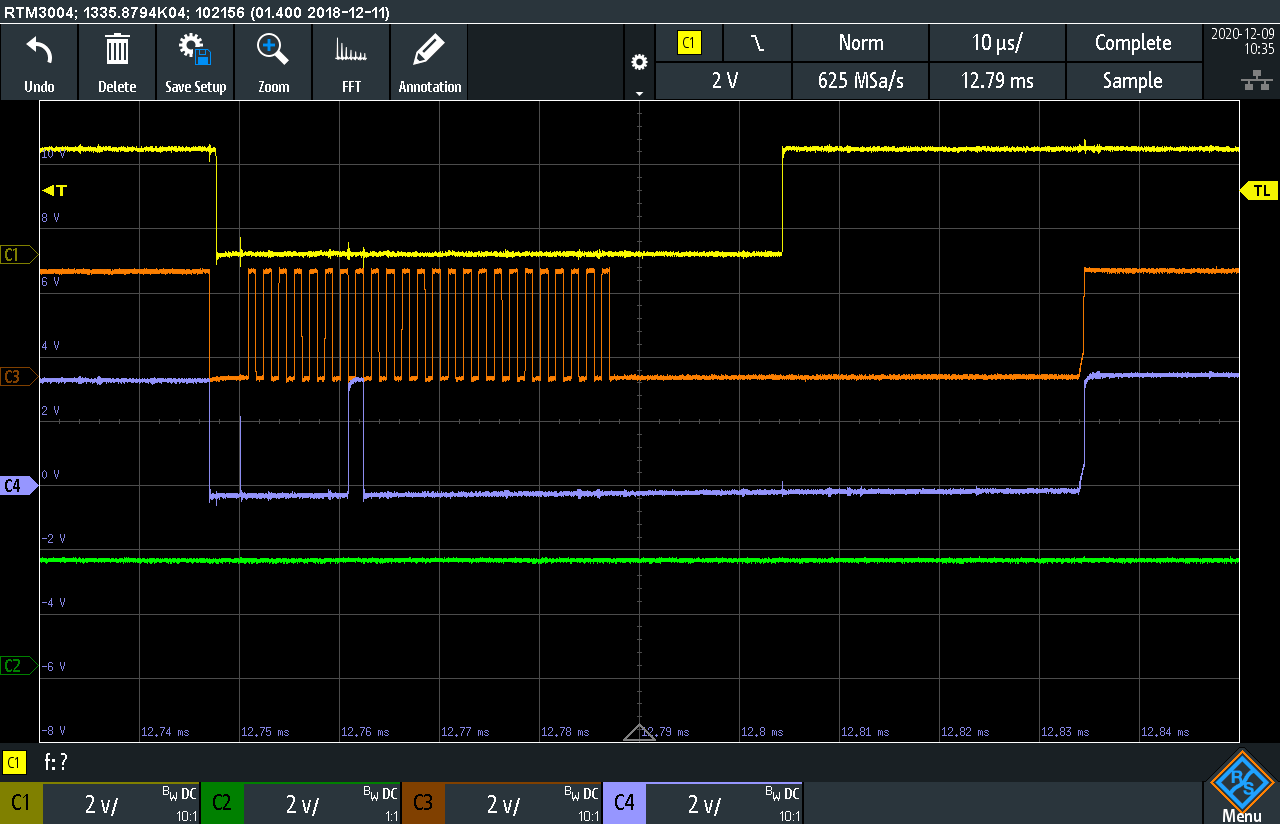
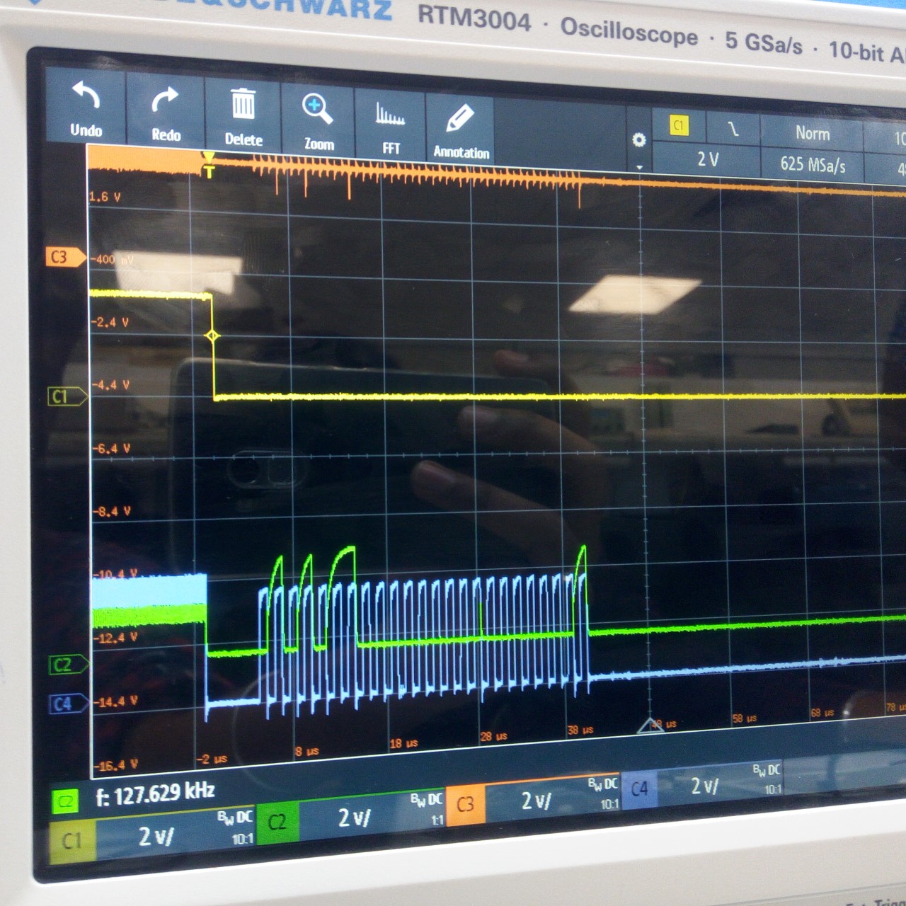
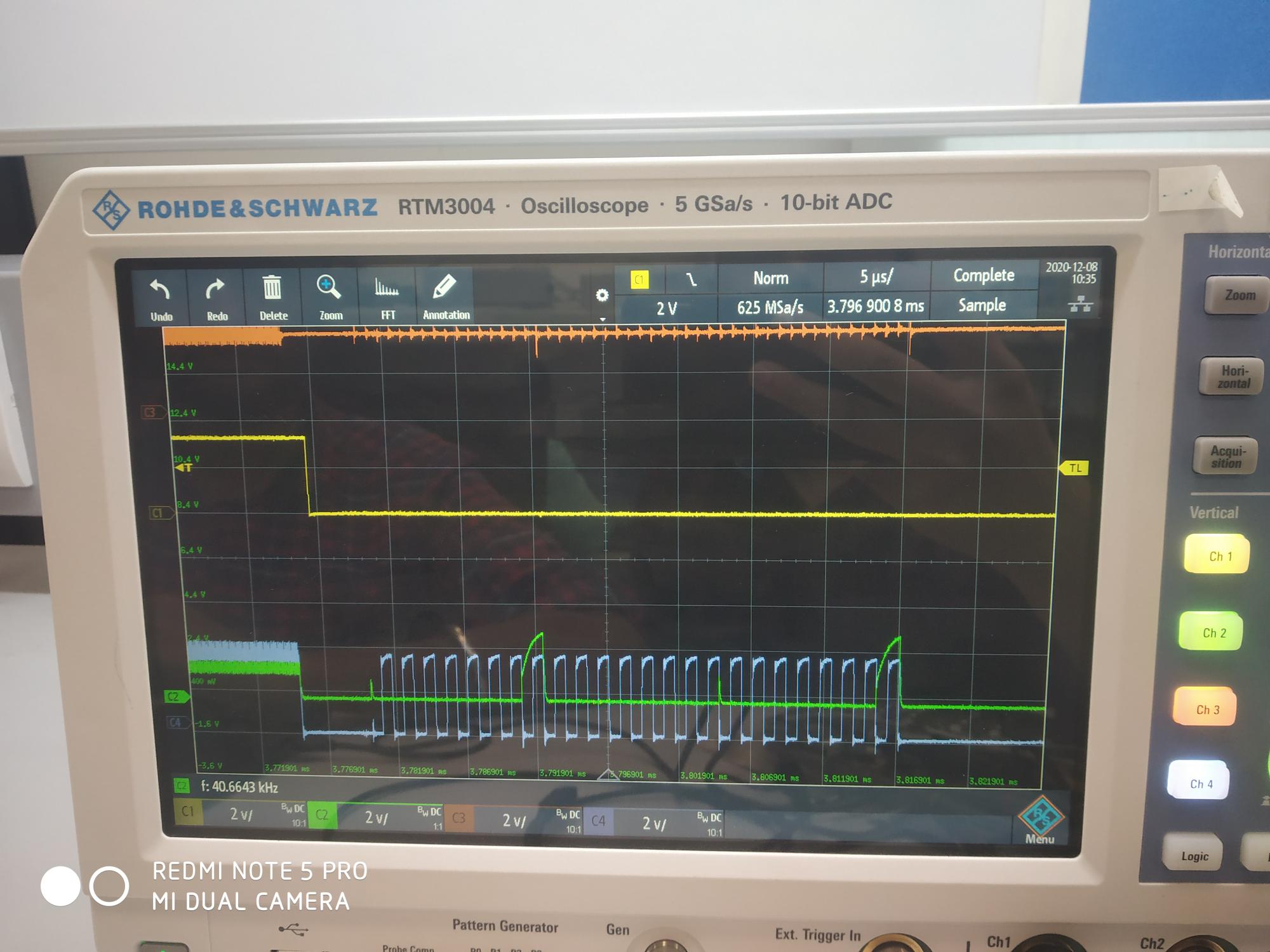
Read DAC register sequence
1. channel 1 ±5 V (dac1_read) No data on MISO


2. channel 2 0V to 10V(dac2_read) MISO data not aligned with clock


Channel details:

c1: chip select
c2: MOSI
c3: MISO
c4: clock

Can you help us to solve this?

Regards,

Manoj

  • Manoj,


    I'm not sure what's happening, but I think you should first address some of the issues in the SPI that you have. I clipped this section out of one of your scope shot images:

    The first thing that I see is that the DIN rises very slowly. I would be worried that DIN rises so slowly that it isn't detect as a high by the time the rising edge of the SCLK comes up.

    The second thing that I see is that there is some significant noise coupling into both the DIN and SCLK signals. If the noise is perceived by device to be an SCLK pulse, then this completely disrupts the SPI communication. It's possible that this noise is EMI or some ground bounce in your system that is associated with some other clock edge in your system.

    Regardless, see if you can clean up these communication issues and then post some new scope shots if you fail to get a response from the device.


    Joseph Wu

  • Hi Joseph, 

    Below are the captured init write sequence and spi read. Still, we are not getting response from the device. 

    Channel details:

    c1: chip select
    c2: MISO
    c3: Clock
    c4: MOSI

    Reset: 56 0001

    Enable and range: 55 1001

    write dac: 01 0000

    Read Dac: 02 0001

    Regards,

    Manoj

  • Manoj,

    A write to a register and reading it back would have been my first test. I'd check the timing, but I don't really see any issues with the waveforms.  However, there are some usually large spikes on DIN, but that wouldn't normally cause problems.

    Just to check are you using any kind of SPI isolation? Regardless, your scope shot should show the communication at the device pin and you want to ensure that the signal reaches the device.

    Just in case, can you share a schematic?

    Joseph Wu

  • Hi Joseph Wu, 

    Thanks for your reply, 

    We have connected two DAC on a single SPI bus(separate CS) through a level translator, previous captured waveforms are on 3V3 side.

    Regards,

    Manoj

  • Manoj,


    Can you try reading back from the control register? Because you've already written 551001, this should set the control register value to 1001. In your last test, you tried to read back from the DAC data register. If you haven't written to that, you would still get back 0000 as a response. Unfortunately you would get 0000 even if the device were dead, because that value is the default. The test would be to try to write to the device and read the same data back. 

    Looking at the schematic, I don't see anything unusual.

    Joseph Wu

  • Hello Joseph Wu, 

    We have already tried to read back of the control register we are getting FFFF as a response, will capture the waveform and send you soon. 

    Regards,

    Manoj

  • Hi Joseph, 

    Attached Write/Read waveforms of control reg for your reference. 

    Write control reg: 55 1001

    Read control reg: 02 0002, No data on C1(MISO)