This thread has been locked.

If you have a related question, please click the "Ask a related question" button in the top right corner. The newly created question will be automatically linked to this question.

ADS1299: Should I change data format if I change V_REF value?

Part Number: ADS1299

Hello TI experts,

My customer now make a new sample with ADS1299, here is one question with Data format.

Before this event, V_REFP is +2.048V / V_REFN is -2.048V. (V_REF=4.096) so the center value is 0(zero), we did not have data conversion at that time.

and this event, we changed V_REFN to -2.5V, V_REFP is still +2.048V. (V_REF=4.548) so i think we should change something in source code for data format.

I captured the part of ADS1299 datasheet below;

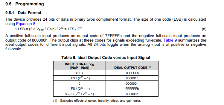
in here I can see that 0V is ideally 000000h, and maybe +2.048V is 000001h. but i am not sure that -2.5V is FFFFFFh, because FFFFFFh is -2.048V in previous event without changes.

then without any changes, we cannot convert more than -2.048V(-2.4V or -2.5V) because we already use full scale in negative.

then I can think 3 ways to solve this problem.

1. modify the value of V_REFN to -2.5 in source code somewhere, so I can change the scale of negative data format (wider). in this case positive and negative scale factors are little different each other. and the position of 0(zero) is same as before. (000000h)

2. modify the value of 0(zero) state in the source, maybe less than 0(zero), then I can use same scale factors from -2.5V to +2.048V. just 0(zero) is not 000000h in hex code.

3. I don't need to change anything, the system will calculate automatically the scale factor even V_REFP or V_REFN changed.

Please check this issue which one is right, and let me know if there are any misunderstanding. Thanks.

Best regards,

Chase

  • Hi Jeong,

    Thank you for your post.

    The analog differential input voltage (VINP - VINN) can span from -VREF/GAIN to VREF/GAIN. When you change the VREF in your design, the LSB of the system also changes, and you need to account for the changes in your source code for data formating (refer to Equation 8 in the datasheet). Your analog full-scale input (FS) now will be 4.548V instead of 4.096V in your previous setup. You can refer to Table 9, which show the ideal output code for different analog full-scale input (FS).

    Thanks.

    -TC

  • Hi TC,

    Thank you for your reply.

    So, if the scale factor decide from GAIN, the answer for my question is 1. (if this is wrong, please tell me.)

    and could you tell me what variable should I change in the source code?

    (ex. V_REFN or LSB or FS or etc....)

    Best regiards,

    Chase

  • Hi Chase,

    Please refer to the ADS129x FAQ listed below for the calculation you need for your source code. Please let me know if you have any questions. 

    How do I convert ADC output codes to volts?

    Thanks.

    -TC

  • Hi TC,

    After you gave me the link for reference, I studied a little the theory in the page.

    now I am little confused, because the link explains obviously V_REF and -V_REF have the same absolute value. (for example, +2.0V and -2.0V)

    1. with the formula "LSB = (2 x VREF)/ Gain / (2^24 - 1)"

    (1) same absolute value +2.0V and -2.0V  --> I can expect the zero value is 000000h.

    (2) different absolute value +2.0V and -2.5V  --> I can expect the zero value is not 000000h, because negative scale factor and positive scale factor is same.

    2. with the "Table 13"

      --> I can expect the zero value is 000000h, whatever the absolute value is.

    (1) if the negative scale factor and positive scale factor is same as +2.0V and -2.0V, the zero value is 000000h.

    (2) if the negative scale factor and positive scale factor is different as +2.0V and -2.5V, the zero value is still 000000h.

    Just let me know, what will be changed if I change the V_REF as +2.0V and -2.5V?

    (1) the value of zero (zero is not 000000h)

    (2) the scale factor (-V_REF/(2^23-1)) -> I think it will become wider.

    please choose one, and tell me if I understand something wrong.

    Best regards,

    Chase

  • Hello Chase,

    TC is on vacation and will be back on Jan 4.

    He will respond to your queries when he returns.

    Thanks for your patience and understanding.

  • Hi TC,

    please update the status if there are any changes.

    Best regards,

    Chase

  • Hi Chase,

    The absolute value of the VREFP and VREFN doesn't matter; the ADC VREF will always be VREF = VREFP - VREFN. In your example, your FS now will be equal to 4.5V (FS = VREF  = VREFP - VREFN) when you have VREFP = +2.0V and VREFN = -2.5V. The ideal output code versus input signal (Vin = InxP - InxN) for the ADC listed in Table 9 will still be valid. When the input signal Vin is equal to 0V, your output code will still be 000000h. In addition to the FS, the LSB will change accordingly with the bigger VREF (1 LSB = +FS/2^23 = +4.5V/2^23).

    Please let me know if this clears up your inquiries.  

    Thanks.

    -TC