This thread has been locked.

If you have a related question, please click the "Ask a related question" button in the top right corner. The newly created question will be automatically linked to this question.

ADS54J60: data are valid but all zero

Part Number: ADS54J60


Hi,

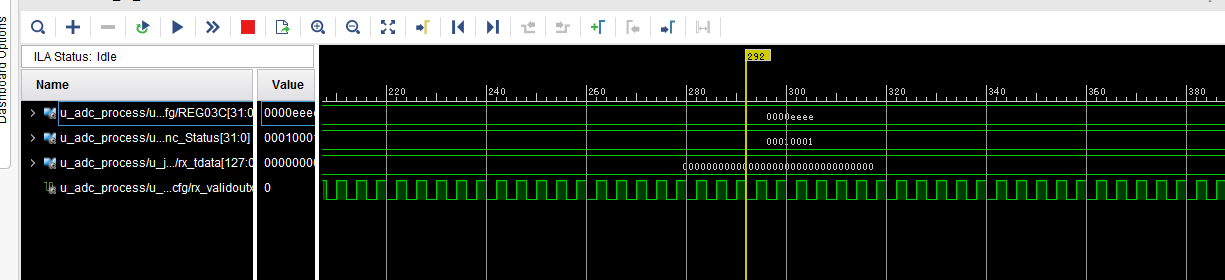
ADS54J60 connected with FMC and  K7,now the JESD204B has no problem,  the PHY data is high and the JESD204B status appears that the data is detected. He used the 4244 mode, each channel appears eeee.

Link Debug status Lane 0
Bit 3: 1 = Start of Data was Detected 
Bit 2: 1 = Start of ILA was Detected 
Bit 1: 1 = Lane has Code Group Sync 
Bit 0: 1 = Lane is currently receiving K28.5's (BC alignment characters) 

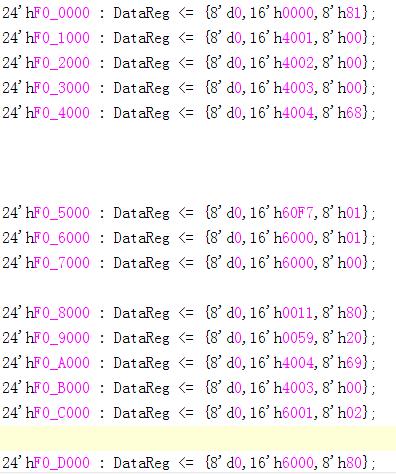
 ads54j60 data Sequence :

Best regards

Kailyn 

  • Kailyn,

    Please use the following sequence for your register writes. You may need to change the value of K as I do not know what your FPGA is set to. Below I have K = 16.

    address                 Data

    0x00                      0x81     //reset

    0x11                      0x80

    0x59                      0x20     // always set bit 5 to 1

    0x4004                  0x68

    0x4003                  0x00

    0x60f7                   0x01   //digital reset

    0x6000                  0x01  // reset 

    0x6000                  0x00  // clear reset

    0x4004                  0x6A

    0x4003                  0x00

    0x6016                  0x02  //JESD PLL mode

    0x4004                  0x69

    0x4003                  0x00

    0x6000                  0x80  // Enable CTRL K

    0x6001                 0x02   // JESD Mode

    0x6006                 0x0F   // K = 16

    0x4004                 0x6A

    0x4003                 0x00

    0x6017                0x40  // PLL reset

    0x6017                0x00    

    Regards,

    Jim

  • Hi Jim,

    The register writing sequence you provided couldn't sync, and the sync pin is not pulled high.

    The customer wrote the register according his previous sequence, the status appears the link has been built, and output data is valid, but he found that the K value of 6006 register may not be written, if wrote 0X80 or 0X00, both of them could link. He captured the data by ILA, the binary value of K is 4(5 frame), F is 3( four octets each frame),N' is 16, N is 14( should be 16bit).  Could you please help to analysis?

    Best regards

    Kailyn


  • Kailyn,

    The customer is getting valid data you mention in first sentence. Why is this an issue then? They need to make sure K is the same value at both the ADC and FPGA.

    What do you mean by "the value of K of 6006 register may not be written"?  Whatever value is written, you should be able to read this back. Did they try to do a read and verify this value was written?

    What do you mean by "if wrote 0x80 or 0x00, both could link"? What was written, and what address?

    There may be an issue with the SPI interface. If they cannot do a valid read, make sure SYREF and sample clock are running before doing any SPI writes and reads. Both clocks are required for proper SPI operation. Also make sure to press the hard reset to the ADC after the clocks are present.

    Make sure the ADC is using the proper power up sequence per the data sheet.

    Regards,

    Jim