This thread has been locked.

If you have a related question, please click the "Ask a related question" button in the top right corner. The newly created question will be automatically linked to this question.

ADS7254: Typo of timing table?

Part Number: ADS7254

Hi Experts,

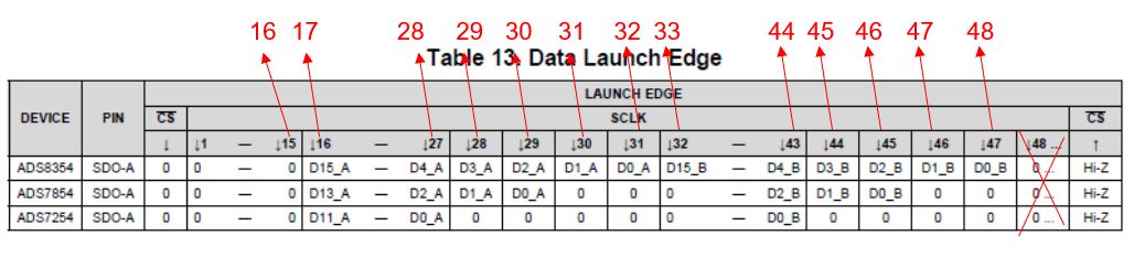
There is a data timing table on page 39. The SCLK timing looks shifted. I am expecting that below is the correct.

Could you please confirm it?

Regards,

Uchikoshi

  • Hello Uchikoshi-san,

    Thank you for your post.

    The Data Launch Edge tables indicate when the data is changed on the corresponding SDO pins. The customer will need to read the data on the next SCLK edge after the bit is changed. So, if data bit 15 is launched on the 16th SCLK falling edge, the customer will read it on the 17th SCLK falling edge. Figure 91 shows the timing diagram for 32-CLK Single-SDO Mode. SCLK edges 17 through 48 are used to read the 32 bits of conversion data (16 bits for each channel).

    Regards,

    Ryan

  • Hi Ryan,

    Thank you for your reply. I am still confusing. This is SPI interface and clock master is MPU(ADS7254 is SPI slave). The point is at which falling clock edge MPU needs to sample the data. For bit "D15-A", figure 91 shows it is 17th falling edge while table 13 shows it is 16th falling edge.

    If figure 91 is correct, we guess table 13 is incorrect.

    Otherwise, when the Data Latch Edge indicates when the data is changed on the corresponding SDO pins, it should be marked as rising edge(↑), not falling edge(↓) in this table.

    Could you please clarify it if I am misunderstanding?

    Regards,

    Uchikoshi

  • Hello Uchikoshi-san,

    I misspoke in my previous reply. When I said "the customer will read data on the next SCLK edge" I meant to say rising edge. You are correct that data cannot be launched and read on the same edge. Table 13 lists the falling edges that correspond to launching each bit on SDO (i.e. when the bit is changed). Therefore, when D15_A is launched on the 16th SCLK falling edge, it should be read by the MCU on the 17th rising rising edge. The delay between SCLK falling edge and next data valid is 20 ns max (tD_CKDO).

    Figure 91 seems to be misleading. Let me confirm with our systems team before we proceed further.

    Regards,

  • Hi Ryan,

    Thank you and understand the clock timing. Please let me know once you can confirm about figure 91.

    Regards,

    Uchikoshi

  • Hi Ryan,

    Can I get any feedback from you? I have to update it to customer.

    Regards,

    Uchikoshi

  • Hello Uchikoshi-san,

    Please use the table as written in the data sheet to indicate the clock falling edge on which the DOUT bit changes. The next clock rising edge should be used to latch this bit by the host controller.

    Regards,

  • Hi Ryan,

    Thank you for your confirmation. I hope that the datasheet will be revised soon.

    Regards,

    Uchikoshi