Because of the holidays, TI E2E™ design support forum responses will be delayed from Dec. 25 through Jan. 2. Thank you for your patience.

This thread has been locked.

If you have a related question, please click the "Ask a related question" button in the top right corner. The newly created question will be automatically linked to this question.

ADS124S08: Data not being returned

Part Number: ADS124S08

Hello,
I am attempting to get a reading from the ADS124S08. The device is being initialized in singled ended mode using ANCOM (pin 1) as the negative input selection (ANCOM is grounded). I am using a raspberry pi 4 and the SPIDEV library in order to send commands to the chip.

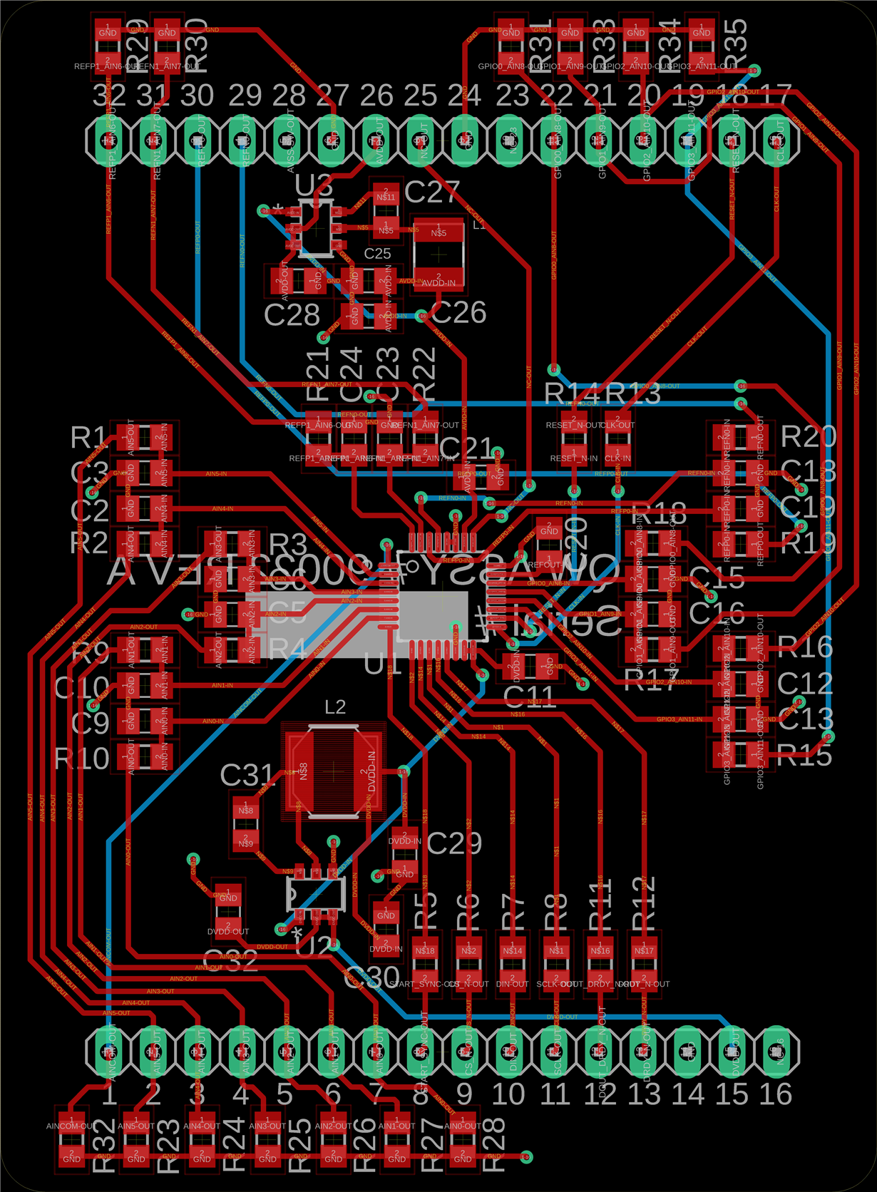
I have attached my python code along with a board layout designed in EAGLE. I have communicated with the chip only through commands and reading the registers. I plan to use AIN0-AIN11 but for testing purposes I am trying to get AIN0 working for now.


-----Declared Registers----

Input Multiplexer Register (0x0C)
Gain Setting Register (0xE0)
Data Rate Register (0x74)
REF (0x19)
IDACMAG (0X00)
IDACMUX (0XFF)
VBIAS (0X00)
SYS (0X11)
OFCAL0 (0X00)
OFCAL1 (0X00)
OFCAL2 (0X00)
FSCAL0 (0X00)
FSCAL1 (0X00)
FSCAL2 (0X40)
GPIODAT (0X00)
GPIOCON (0X00)

import spidev
from time import sleep
import os
import sys

#clear terminal
os.system("clear")
sys.tracebacklimit = 0  #suppress traceback errors

#----------Initialize Variables/Commands----------#
SPI_BUS = 0         # spidev0
SPI_DEVICE  = 0     # spidev0.0
SPI_CLOCK = 125000  # 125 kHz limit

# setup SPI
spi = spidev.SpiDev()
spi.open(SPI_BUS, SPI_DEVICE)
spi.max_speed_hz = SPI_CLOCK
spi.mode = 1

NOP = 0x00          #no operation command
WAKEUP = 0x02       #wakeup command
PWRDWN = 0x05       #powerown command
RESET = 0x06        #reset command
START = 0x08        #start command
STOP = 0x0A         #stop command
RDATA = 0x13        #read data command

#function to handle the SPI communication and print the command to terminal
def output(varName, cmd):
    print(varName)
    print("    Sent to ADC --------->", cmd)
    data_in = []
    data_in = spi.xfer(cmd, 100000)
    print(f'    Received from ADC ---> {data_in}')
    print("------------------------------------------------------")
    sleep(0.3)

try:
    #----------Initialize ADC send----------#
    output("WAKEUP - 0x02", [NOP, WAKEUP])      #wakeup ADC
    output("RESET- 0x06", [NOP, RESET])         #reset ADC

    output("Declare PGA, Data Rate, Reference, Exciation Registers",[0x43, 0x02, 0xE0, 0x74, 0x19]) # Start at 3rd register and declare registers 3,4,5
    output("Declare System Control Register",[0x49, 0x00, 0x11])    # declare register 9

    output("Input Multiplexer to 0x1C",[0x42, 0x00, 0x0C])
    
    output("START - 0x08", [START])             #start ADC
    n = 0

    while True:
        output(f"[{n}] Status",[0x21,0x00,0x00])
        output(f"[{n}] RDATA COMMAND",[0x12,0x00,0x00,0x00,0x00])
        n = n + 1
        sleep(3)
        
finally:
    print("Stopping...\n")
    output("STOP", [STOP])
    output("PWRDWN", [PWRDWN,NOP,NOP]) 
    spi.close()

Read status bit 0x21 (decimal 33) sent to adc. 0x80 (decimal 128 or binary 0b10000000) returned. This is due to not clearing the FL_POR flag in the status register for testing. The SENDSTAT bit in register has been turned on. When the RDATA command is sent I should be receiving 128 followed by 3 bytes of information. I have only received zeros back every time the RDATA command is issued.

Any help would be appreciated. If more information is needed please let me know.

  • Hi Alex,

    Welcome to the E2E forum! I'm not sure what the timing of your delay function but you need to make sure that there is sufficient delay between sending RESET command and the write register command.

    Also, I would suggest monitoring your communication with an oscilloscope or logic analyzer to make sure that the communication is correct.  The CS pin must be held low throughout the entire communication transaction.  This means that for multi-byte commands, such as writing to the register, the CS pin cannot toggle between bytes or the communication will cancel on the rising edge of CS.  Please send any scope or logic analyzer shots for me to evaluate.

    I would try simplifying things as much as possible to help in troubleshooting.  An example would be to leave the internal reference powered even in power down mode, and use the internal oscillator instead of the external clock.  Make sure that RESET is pulled high and that all required supply voltages are present.

    You are operating in single conversion mode.  Monitor DRDY output with a scope to see if DRDY makes a transition from high to low following the START command.  At 20sps, the DRDY should make the transition from high to low which signals end of the conversion and the result is ready to be read from the device.  Make sure that you wait at least 50ms (period for 20sps) for the conversion to complete before attempting to read the data following the issue of the START command.

    Best regards,

    Bob B

  • Hi Bob,

    Thanks for your quick reply! I'll do my best to answer your previous questions and then supply some oscilloscope shots.

    1. I'm not sure what the timing of your delay function but you need to make sure that there is sufficient delay between sending RESET command and the write register command.
      1. My current delay between each command is 1 second. I have gone up to 3 seconds between each command but the result is always the same.

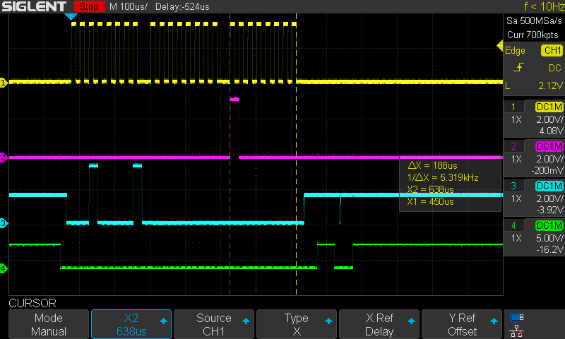
    2. The CS pin must be held low throughout the entire communication transaction.  This means that for multi-byte commands, such as writing to the register, the CS pin cannot toggle between bytes or the communication will cancel on the rising edge of CS.  Please send any scope or logic analyzer shots for me to evaluate.
      1. Channel 1 is the CLOCK. Channel 2 is MISO. Chanel 3 is MOSI. Chanel 4 is CS. In the picture below, I am reading register 1 (0x21), reading only 1 register (0x00), and clocking for the return byte from the ADC (0x00). There is a return of (0x80). This return is expected as I am not clearing the FL_POR bit in the status register. The CS pin is held low during the duration of the commands. This is using the external clock on the raspberry pi.


    3. I would try simplifying things as much as possible to help in troubleshooting.  An example would be to leave the internal reference powered even in power down mode, and use the internal oscillator instead of the external clock.  Make sure that RESET is pulled high and that all required supply voltages are present.
      1. I have changed the internal reference to be powered on even in power down mode but this did not have a different effect on the output. The reset pin is being pulled high at all times. I tried changing over to the internal oscillator but this seems to break down the communication between the raspberry pi and ADC because the clocks are no longer synced. I am sure I am not using the internal oscillator correctly and am not sure how to proceed with that. For the time being, I have switched back to using the clock from the raspberry pi at 125kHz.


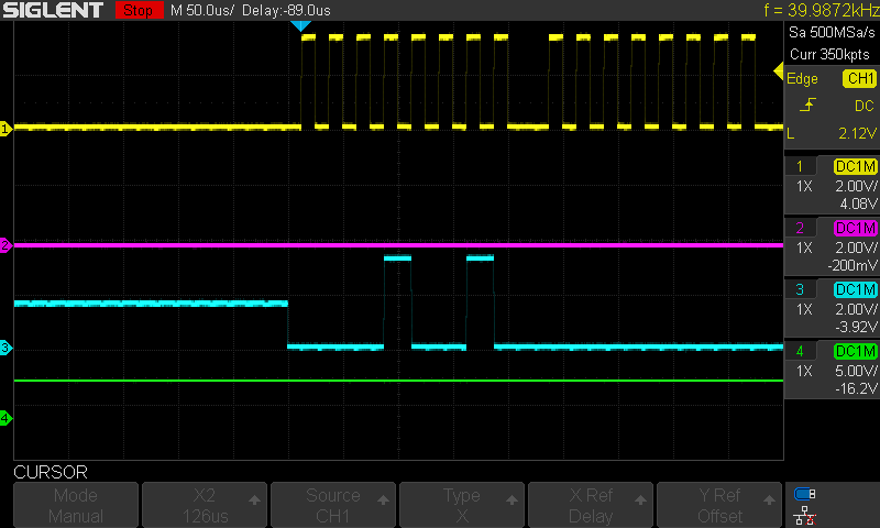
    4. You are operating in single conversion mode.  Monitor DRDY output with a scope to see if DRDY makes a transition from high to low following the START command.  At 20sps, the DRDY should make the transition from high to low which signals end of the conversion and the result is ready to be read from the device.  Make sure that you wait at least 50ms (period for 20sps) for the conversion to complete before attempting to read the data following the issue of the START command.
      1. Channel 1 is the CLOCK. Channel 2 is MISO. Chanel 3 is MOSI. Chanel 4 is DRDY. The delay time between commands is 1 second. DRDY never appears to go low after the START command is issued.

    Thanks again for your help. Hope to hear from you soon!

    -Alex

  • Hi Alex,

    I think there may be a misunderstanding about what I was saying for the clock.  There is no synchronization between device clocks for the ADC master clock.  I was not talking about the SCLK but rather the master clock of the ADS124S08.  The internal oscillator operates at a nominal external clock frequency of 4.096MHz.  To use the internal oscillator, you need to set the CLK pin (17) low otherwise you must provide a clock of at least 2MHz up to a maximum of 4.5 MHz at the CLK pin.  Also, you would need to set the register setting appropriately for using the external clock.

    The external clock will determine the conversion rate of the ADC.  For example, if you applied an external clock of 2.048MHz to the CLK pin, then it will take twice as long for the conversion to complete as compared to 4.096MHz.  The conversion result timing will scale with the input clock frequency.

    To simplify operation I would set the breakout board connection on pin 17 to logic low on power up.  For register 0x04 setting, make sure bit 6 (CLK) is low which is the default setting to use the internal oscillator.

    Best regards,

    Bob B

  • Hi Bob,

    That was it! I didn't understand the SPI clock VS the internal clock. The internal clock has been turned back on and I am now receiving data. Thank you for all of your help!

    -Alex