This thread has been locked.

If you have a related question, please click the "Ask a related question" button in the top right corner. The newly created question will be automatically linked to this question.

ADC3444: Register 0x25 LVDS Swing

Part Number: ADC3444
Other Parts Discussed in Thread: CDCLVP1102, , LMH2832, LMZ12003

What is the register mapping for the LVDS swing? The data sheet doesn't provide any information. I have some spurs due to the digital signals and I have tried simply all 256 values. I have found a setting, where the spurs are reduced, but now the data transfer has sometimes errors. I need a description for an advanced optimization.

  • Hi Volker,

    I am looking into the details of the LVDS Output swing register, and will get back with you shortly.

    Have you utilized the digital test patterns (Ramp and other patterns, see page 63 of datasheet) to validate the digital interface in the FPGA?

    Best Regards,

    Dan

  • Hi Dan,

    thank you so far, I have checked the correct transmission with the patterns. It works for the normal setting. Perhaps with lower swing the phase of the PLL in the FPGA must be optimized. The board contains two ADC3444, the input clock is distributed by a CDCLVP1102, there are some LMH2832 in front of the ADCs(besides mixers,LNAs and filters). Perhaps some coupling into the power supply occurs, also I have used separate LDOs and ferrite beads. The distortion is mainly on the first ADC, the other ADCs(2-4) of the chip are okay.

  • Hi Volker,

    Is this distortion happening on Channel 1 (CHA) of both ADC3444s, or just one of the two ADC3444s (meaning that 7 of 8 total ADC channels are not distorted)?

    If the test patterns are coming through ok on CHA (one with distortion) of the ADC3444, then this is likely an analog issue, as you mentioned.

    What is the nature of distortion/spurs that is being seen? Are they harmonic spurs of the analog input frequency? Are the spurs present when no analog input is applied? Are you performing an FFT to see the spurs? Are you able to probe this analog input to verify that there are not spurs present at the ADC pins?

    Please share an image of spurs and ADC/signal chain schematic.

    Best Regards,

    Dan

  • Hello Dan,

    yes, 7 of 8 are okay, sometime there are peaks, but not in a grid like in the figure below(32K FFT). The second figure shows the second channel.

    The lowest figure is channel 1 with LVDS swing set to 252. The peaks are slightly decreased. This is just noise with full amplification, the noise is shap by the bandpass.

    It could be some distortion by digital signals or maybe a switching frequency of a power converter, but there is always an additional LDO for all parts.

    The schematic is quite huge and I don't want to publish it, but perhaps you have an idea.

  • Hi Volker,

    It is difficult to say what exactly is causing this noise on only one channel of the ADC. Are you using the VCM output of the ADC to set the common mode for the amplifiers? Is the common mode voltage correct on the analog input pins for the noisy channel?

    Can you please try powering down the three good channels on the ADC with the one noisy channel and see if this effects the spurs? Can you also please ensure that a hardware reset is being performed before the ADC is programmed?

    Best Regards,

    Dan

  • Hello Dan,

    i is a good idea to power down the other converters, A reset is performed at the start. Perhaps there is a relationship with the unterminated frame clock. I will solder a resistor on the board. I couldn't connect the second frame clock to the fpga because of the number of limited pins at the HSMC connector.

    Could you find a register decription for the swing?

    Thank you so far, it is a complicated search.

  • Hi Volker,

    The details of this register are actually in page 63 of the ADC324x datasheet (will work on getting this updated in the ADC344x datasheet). As you can see from the table, writing values other than default (0x00) will reduce the LVDS output swing.

    Hope that helps.

    Best Regards,

    Dan

  • Thank your for your support, I will continue the debugging.

  • Hi Volker,

    Is it possible to disconnect the analog frontend (mixers, LNAs, etc) and only measure the ADC FFT performance?

    I would try this test and make sure the noise is not coming from the preceding components that connect to the analog inputs of the ADC.

    Terminate the ADC analog inputs to AC coupled ground and measure the output spectrum and let us know what you find.

    Regards,

    Rob

  • Hi Rob,

    thank you for further interest.

    There are several test points in the receive path. It is possible to connect a small pcb with balun by pin headers after desoldering coupling capacitors to the normal path. This allows to connect a signal generator over the small balun board.

    Unfortunately I have been interrupted by some other work so that it can't perform further testing immediately.

    I have already seen some spikes at the output of the variable gain amplifier on a spectrum analyzer after desoldering the connection to the A/D converter, but could not identify the source of the periodic peaks.

    Additional bypass capacitors to several components, other inductors for mixer biasing or replacing the VGA with a new component didn't help. If I have news, I will post it.

    Best regards,

    Volker

  • Hi Volker,

    The "spikes" that you see are from the ADC's analog inputs, assuming you are probing on the VGA that is still connected to the ADC. Correct?

    If so, then those spikes are the ADC's sampling switch charge injection that can be seen on the analog frontend.

    You will see it as well, if you do the balun experiment....

    Doing the balun experiment is a good idea btw, to see if the frontend noise is, from the FFT spectrum plot above, is again coming from the VGA/frontend.

    otherwise, completely disconnecting the analog frontend signal chain would also show this.

    Regards,

    Rob

  • Hello Rob,

    I think that I have found the issue: It is probably the switching frequency of a power regulator, a simple switcher LMZ12003, which is placed to close to some coils of an IF-Filter in front of the ADC input. If I hold a ferrite bead for a cable over the switching regulator, the peaks are gone. If I place a finger on the regulator, the peaks grow. The distance to the other filters and receive channels is larger, this explains the behavior.

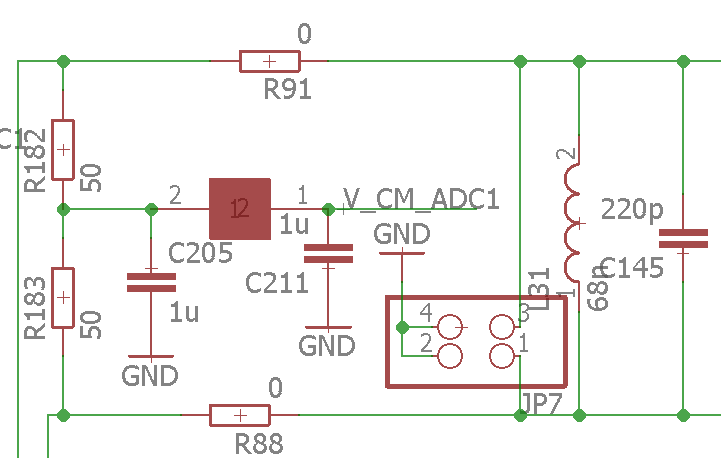
    Before I have found this, I have replaced a ferrite bead by a 0Ohm resisistor at the ADC input stage. I have observed no difference.In  the schematic of the evaluation board there is also a 0Ohm resistor and two 0.1muF bypass capacitors.Below you can see the schematic of my input stage.

    Can you tell me, if you have made any investigations about the optimum configuration?

    Best regards,

    V. Winkler