This thread has been locked.

If you have a related question, please click the "Ask a related question" button in the top right corner. The newly created question will be automatically linked to this question.

ADS8681 Enquiry on output pin of ADC in TINA

Other Parts Discussed in Thread: ADS8681

Hi,

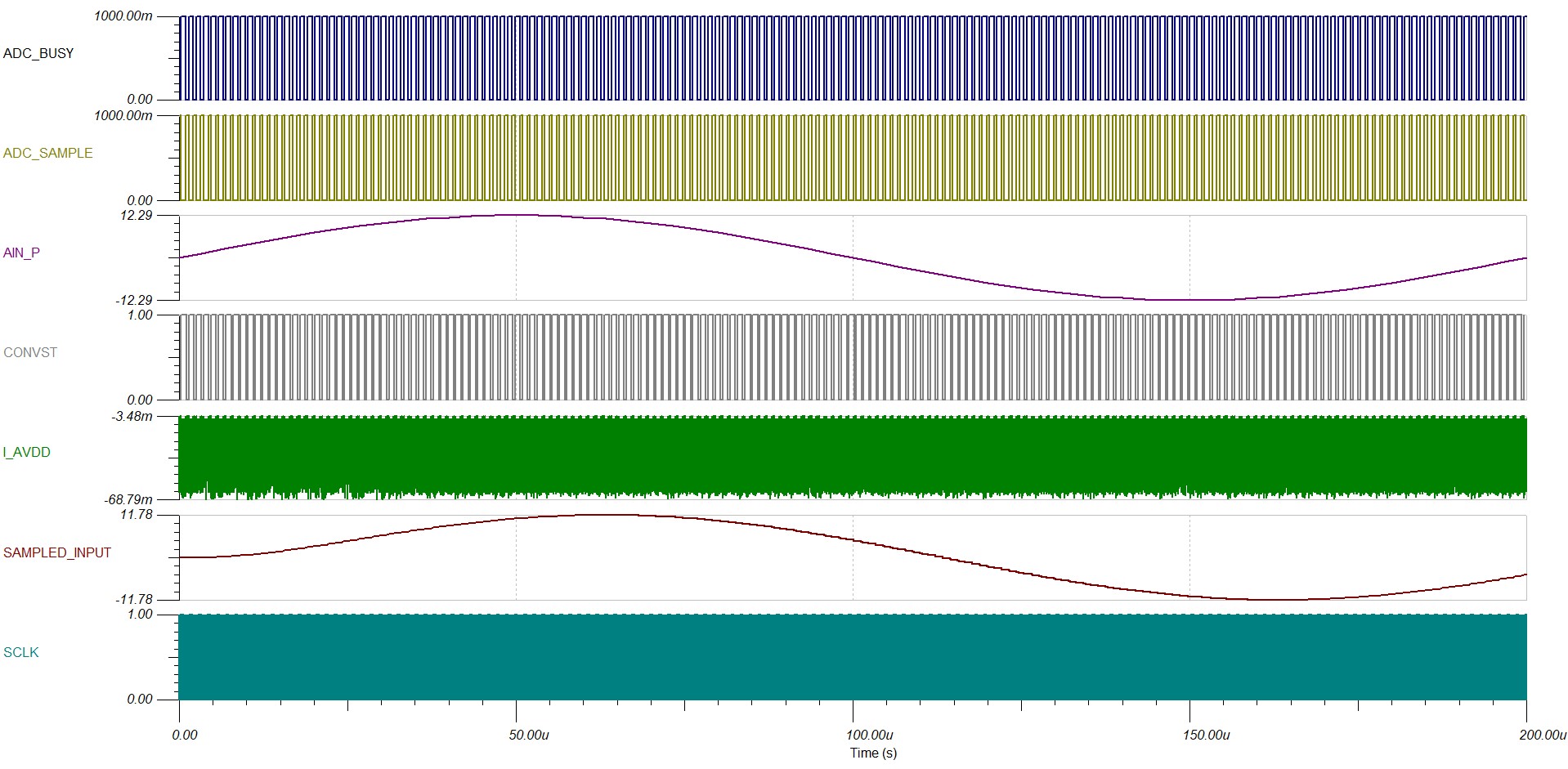
May I know which pin is the output (the signal that has been sampled) of ADC?

Is it "ADC_SAMPLE"?

Thanks

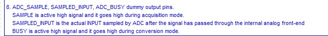
Actually, I don't really understand these terms found on the TINA reference design file. I can't find these terms on ADS8681 datasheet as well.

Can explain more in details on these terms?

Thanks

  • Hi David,

    The "Sampled_INPUT" is the output which is the sampled signal from the input sinewave signal applied on the "AIN_P". See the transient simulation result below.

    The simulation circuit in this reference design is a simple approach to show how the ADC is working by showing the conversion and acquisition operation, also some key parameters have been modeled on the device so that you can see a dynamic change during different operation phases, for example AVDD current (I_AVDD). 

    Best regards,

    Dale

    Zoom in: