This thread has been locked.

If you have a related question, please click the "Ask a related question" button in the top right corner. The newly created question will be automatically linked to this question.

DAC81416: dac81416

Part Number: DAC81416

For output 0~20V, each channel is output to the maximum 25mA application scenario

1. Does it mean that the supply current of VCC and VSS should be at least 25x16=400mA

2. How should the power consumption of DAC be estimated?Whether the power consumption of DAC is Power Supply Headroom x 25mA x 16 regardless of the output voltage?If so, does it mean that the higher the supply voltage, the greater the power consumption of the DAC?

3 output 0~20V in order to achieve the accuracy of 10mV, what is the requirement of the reference voltage?The EVM is REF5025AID with 0.1% accuracy, is it only possible to achieve the accuracy of 2.5 x 0.1% x (20/2.5) =20mV?

4. When the output accuracy reaches 10mV, whether DC/DC scheme can be adopted for VCC and VSS and to what extent will the output be affected?Do you care about AC PSRR and DC PSRR?

5. If there are multiple DAC on the board, is it necessary for each DAC to adopt independent power supply to reduce mutual interference?

6. Considering the above problems, if the input voltage is 24V+/-5%, for multiple DAC on board, such as 8 DAC, is there a suitable power supply scheme recommended by TI?

  • Hi,

    Please find my answers below.

    1. It has to be 400mA + Supply current of DAC81416, in this case 400mA + 25mA(max Icc) = 425mA

    2. Think of this as an operational amp driving the outputs. Power dissipation in DAC81416 = (Vcc – Vss) * Icc + (Vcc – Vo) * Iout (assuming current flowing out of DAC) So, it depends on supply voltage, Output voltage and load current. Similar way you can calculate when the DAC is sinking current.

    3. You may need to use the higher accuracy version of REF5025, 0.05% if there is no calibration is planned for this design. If gain error due to DAC and reference are calibrated, you don’t need to worry about this specification. What you really need to look into is the tempco’ s of the reference and DAC.

    4. Can you please elaborate this question, I didn’t understand what do you mean by DC-DC scheme? You mean DC-DC power supply for VCC and VSS? We do care about PSRR for this device. See the datasheet for more information

    5. Not necessary, please follow proper layout guidelines to avoid mutual interactions and coupling between the devices.

    6. I am assuming you are looking for 0 to 20V output with 24V supply with VSS  = 0V right? Also please note that single 0-24V supply might cause problems with low codes near zero. This is because the output buffer will not drive to ground unless a bipolar supply is used. If this is a concern, you would need to use a supply with VSS set to a negative voltage

    Regards,

    AK

  • DC-DC is a buck and boost regulator. It is a buck and boost regulator.

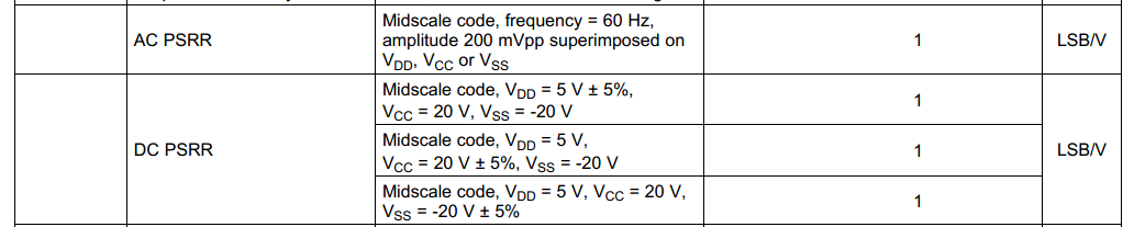
    According to the manual, the ripple caused by the power switch mainly depends on AC PSRR, and DC PSRR is the main variation of the power supply. 1LSB is about 0.3mV. Does it mean that the output precision of 10mV does not require high demand on the power supply, and the switching regulator is completely OK? 


    6. The design of the input voltage of the power adapter is 24+/-5%, considering the VCC and VSS power supply, VSS is prepared to use negative voltage.Combined with question 1 and 5, if the 8 DAC are not supplied separately, the required current is quite large, that is, 425mA x 16 = 6.8A. I'm afraid LDO is not A reasonable solution, and there are not many options for switching regulators with such A large current, especially the negative voltage.So I want to ask the recommended scheme and device.

    Current plans are:

    A. 24V+/-5% input using LDO to generate a voltage of around 22V as VCC (see chip capacity may require multiple)

    Combined with question 4, is this level of LDO very necessary?

    B.  24 V to 5 V (for VAA and VDD), 5 V  - 1.8 V as VSS (see chip may need more than one)

     for 5 V - 1.8 V, website TPS63710DDR moutain, but only 1 a current, put eight means, want to ask whether there is a more suitable scheme?

  • Hi,

    LDO is not necessary if you can provide sufficient filtering for the power supply from DC DC converter.

    Also for anything related to power supply design or recommendation, please post the same to POWER e2e group, they will be in a better position to suggest suitable parts based on your requirements.

    Regards,

    AK