This thread has been locked.

If you have a related question, please click the "Ask a related question" button in the top right corner. The newly created question will be automatically linked to this question.

ADS8920B: Corrupt data in QSPI mode.

Part Number: ADS8920B

Hi.

We are using the above converter in QSPI mode with the data being read by an FPGA.

There is a very odd fault in that the data lines all read the same value (either all ones or all zeros depending upon Vin) in each of the four nibbles that are read.

All other bits work correctly resulting in steppy data of xxFx or xx0x only.  We have verified this on a 'scope and it is consistent.  Vref = 4.5V, RVdd = 5.0V, DVdd = 3.3V. SPI clock = 16MHz, conversion period = 2us.

RVS is used to start the data transfer and all SPI timing restrictions have been observed.

Unfortunately I don't have another chip right now to check if this one is damaged, but there is no reason it should be.

  • Hello Graham,

    Which QSPI mode are you specifically using?  Would it be possible to capture the waveforms and attach?

    I have seen odd behavior if the bypass capacitors are not properly placed and routed near the ADC, but not this specific issue.  Are you looking at this on a TI evaluation board, or your own hardware?

    Regards,
    Keith Nicholas
    Precision ADC Applications

  • Hi Keith,

    Thanks for your very quick reponse.  Here is the information you requeated:

    ADC setup is as follows:-  (Register no, value)

        FPGA_ADC_Write(0x0C, 0x0C);
        FPGA_ADC_Write(0x04, 0x00);
        FPGA_ADC_Write(0x08, 0x00);
        FPGA_ADC_Write(0x20, 0x01);
        FPGA_ADC_Write(0x30, 0x00);

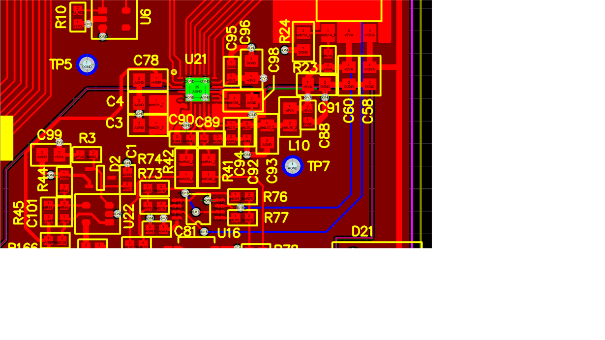
    Design is our own board, relevant area below.

    Brown is an inner power layer, green is an inner ground layer.  Both are partitioned under the ADC between analog and digital domains. The two ground plains are effectively linked by the ground pad of the ADC.  The power plains are independant.

    We have also noticed that VREF is being hard driven (via 22R) by a precision opamp which might be an issue for the ADC as the opamp is powered from 12V.  I have found that a 1k source resistor is recommended and wondered is this might stress the ADC at power up or during operation.

    I will try and get a scope trace later but all clocks and data were within the RVS low period.

  • Scope trace of RVS, SPI Clock and a data line.

  • Hi Graham,

    I do not see any issues with what you provided.  Based on your timing waveform, I assume you are reading data back data during Zone 1, when the device is in acquisition mode?   Can you confirm that the hold time requirement between the 4th clock falling edge and the rising edge of /CS is met, minimum of t-ht_CKCS=7nS?  (Refer to Figure 3)

    Regarding your question on the VREF input, if this input voltage is exceeded, it can cause the device to behave unpredictably.  This can occur during power-up if there is a voltage applied to this input before the RVDD voltage has had a chance to ramp up, or, if the voltage on this pin exceeds RVDD+0.3V (5.3V) after power-up.  Increasing the series resistance will provide some additional protection to these fault events, if they are occurring.  In addition, adding a series resistor of 1k-10k on this pin also creates a low pass filter with the REFIN capacitor, reducing the noise from the external reference, which is why we typically recommend including it.

    I would suggest increasing the 22ohm resistor to 10kohm to see if this helps.

    Also, if you can get another board working, it would be good to confirm that the part itself is not damaged.  If more than 130mA flowed through the REFIN pin at any point, the part could be permanently damaged.

    Regards,
    Keith

  • Sorry, in the previous trace, it was CSn not RVS which does meet the timing requirement.

    I have got the second board working which does something slightly different but it is still not correct.  I tried a10k in series with Vref but it made no difference.

    This trace shows RVS.

  • Hi Graham,

    I do not see anything wrong so far.  Here are a few more things to check.

    1.  Short the input pins together and drive the node to Vcom=1/2*Vref, or 2.25V in your case.  If there is an issue with the input amplifier, or the reference, this should help.

    2.  Have you measured the SDO pins on a logic analyzer or scope to verify that the faulty output code corresponds to the code that you capture with the FPGA?  I have seen some cases where the ADC generating the correct code, but there was some sort of error in the capture of the data.

    Could you share an image of the schematic showing the ADC, input amplifier, and reference?

    Regards,
    Keith

  • Hi Keith,

    If you can contact me privately by email to the account address, I will send you a schematic.

    On the schematic, we have tried just feeding a signal straight into U20 disconnecting U13 and still see the same problem.  I have my second board fixed now and that shows a similar (though not identical) problem.  I am waiting for some more parts to arrie from your frozen Texas warehouse and will try changing the part whilst adding a series resisitor in Vref in case this has caused damage.

    As I said before, the data is real as we have seen it on the 'scope, and when we put the ADC in test mode, all bits seem to work fine.

    Regards,

    Graham

  • Hi Graham,

    I will contact you directly at your myTI email address.

    Regards,
    Keith