This thread has been locked.

If you have a related question, please click the "Ask a related question" button in the top right corner. The newly created question will be automatically linked to this question.

ADS7945: Please review the schematic

Part Number: ADS7945
Other Parts Discussed in Thread: , ADS7946, INA210, INA229, INA240

Hello TI experts,

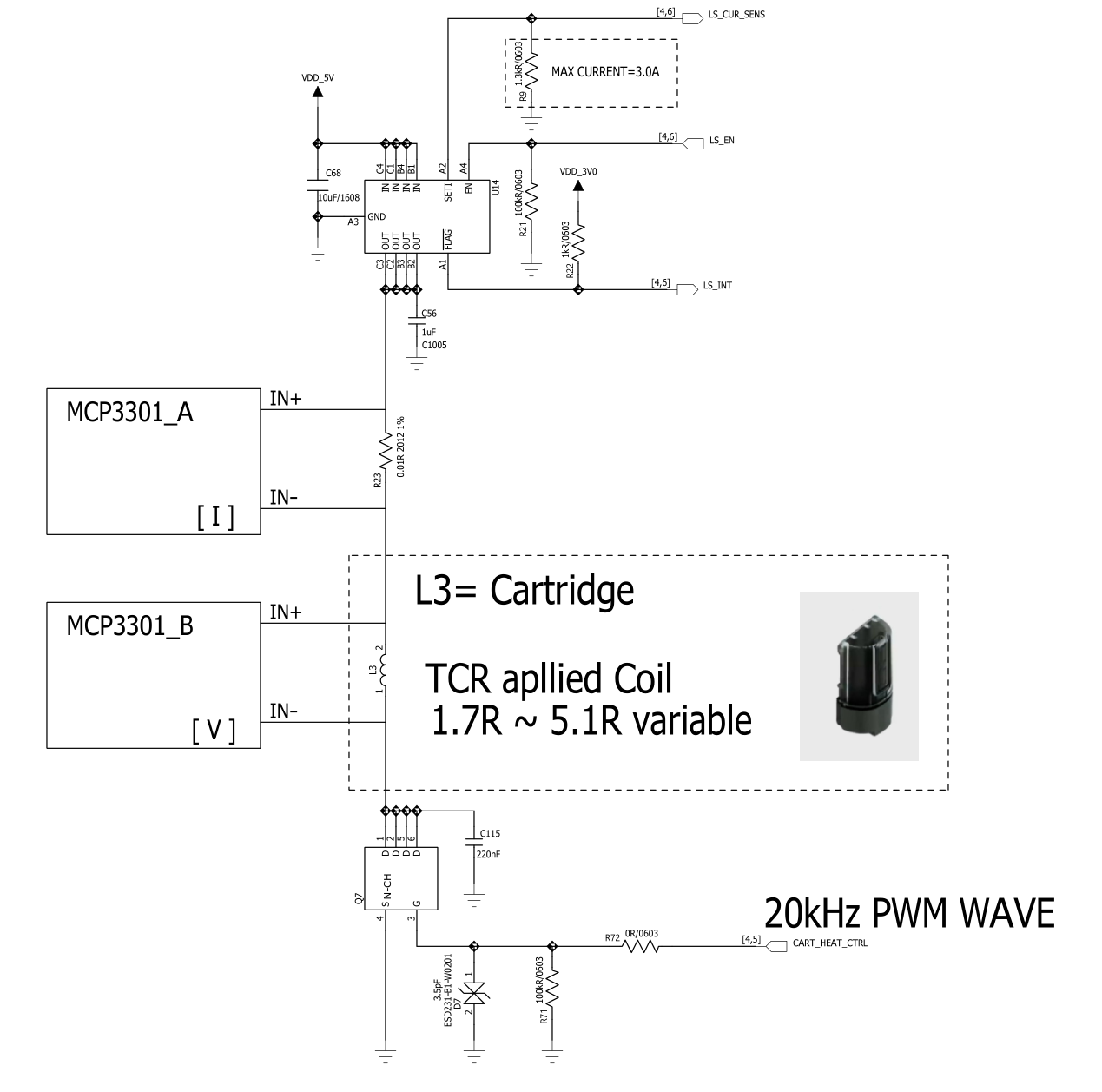
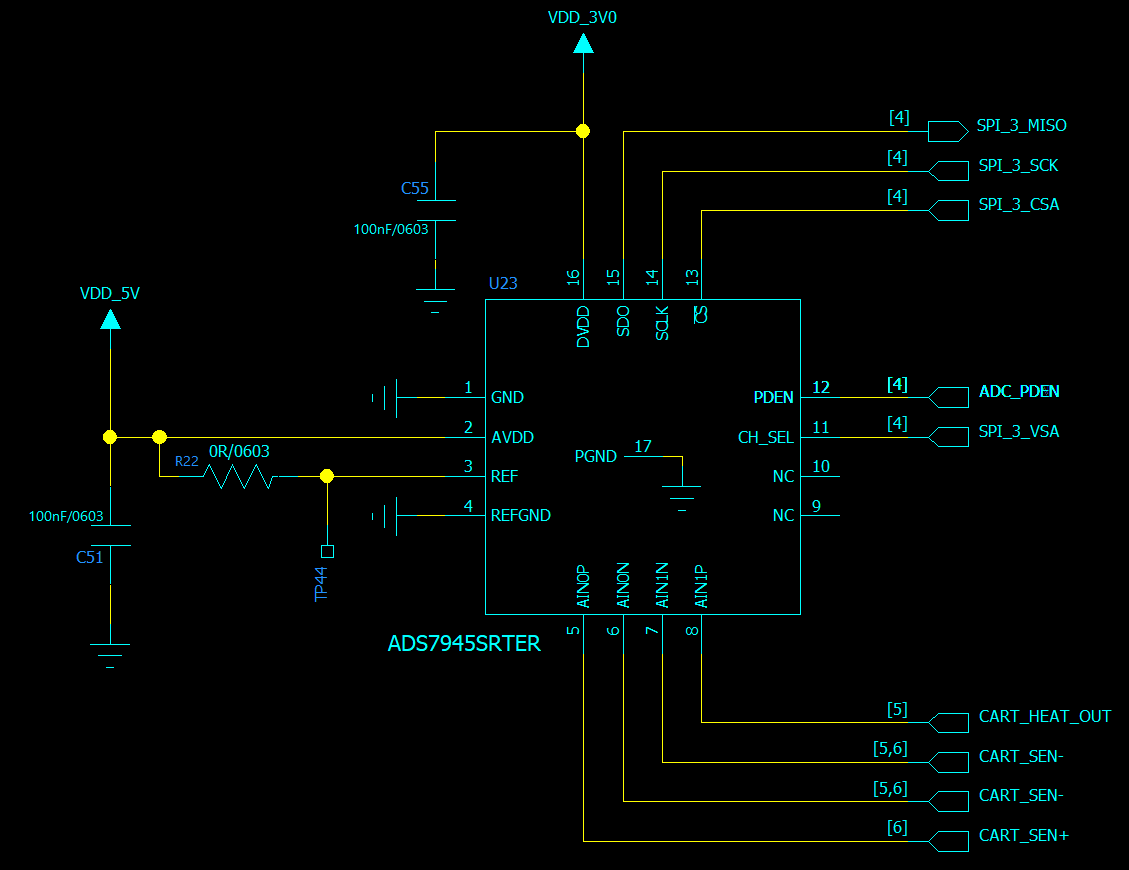
my customer considers ADS7945 for their product, they drew first schematic.

please review the schematic below;

they want to use 0V~5V PWM signal as input, and 3.0V for output digital signal.

so please check the voltage of AVDD, REF, DVDD are right.

and i have one more question, about power down mode in page 30 of datasheet.

in datasheet, "Note that the device looks at the PDEN status only at the CS rising edge"

then what is the first sequence? PDEN to 1 and make rising edge for \CS next? or first make rising edge for \CS and PDEN to 1 next??

how about from power down to normal operation? should we follow PDEN to 0 and \CS falling edge?

please give me a detailed description about this. Thank you.

Best regards,

Chase

  • Hello Chase,

    The basic connections you've shown to the ADS7945 are correct, but there's admittedly not much shown around the device in terms of what's connected to the inputs.  Here are some notes based on the schematic and your comments.

    1.)  We recommend a separate reference decoupling capacitor (100nf - 1uF) connected directly between the REF and REFGND pins.  Currently this capacitor is shared with AVDD.  Extra inductance in the reference capacitor connections will reduce performance due to ringing on the internal reference circuitry when the inputs are converted. 

    2.)  Supply voltages for AVDD, REF, and DVDD are fine for a +5V analog system with +3V digital I/O levels.

    3.)  If running at full speeds it's likely that the performance would improve with an input buffering circuit that will help charge/discharge the internal sampling capacitor during the acquisition period.  For more details on the theory behind this take a look a these videos.  We recommend you reference the information in the videos over the datasheet applications section as the videos have the most refined versions of the design process versus what was available when this product released.

    https://training.ti.com/node/1139106?context=1139747-1140267-1128375-1139106

    4.)  In regards to the PDEN pin, basically there's an latching circuit that sets the state for the internal power-down state which is triggered on the rising edge of /CS.  No internal changes occur to the Power-Down state until the PDEN state change is latched into the internal state machine by the rising edge of /CS.  

    So, yes, you'll need to change the PDEN pin logic state, before the /CS signal rises to toggle between power-down and active modes.  There are some examples in Figures 83-85.

  • Hello Collin,

    Thank you for your reply.

    Now they test their concept with ADS7945EVM-PDK, and there is some problem.

    1. the schematic is as below, we replaced MCP3301B_B to ADS7945EVM-PDK.

    2. they used 5V for AVDD and Vref.and DVDD is 3.0V for SPI communication in ADS7945EVM.

    3. The PWM signal, Drain pin of Q7 is changed to 10% to 90%. high voltage is 5V.

    4. If we put 5V in A0(+), minus value is created in A0(+)/A0(-) differential voltage mode. (see left of the picture below)

        if we put 4.2V in A0(+), minus voltage is not created in A0(+)/A0(-) differential voltage mode. (see right of the picture below)

    5. What is the reason that we get minus value if we use 5V in A0(+)?

    we tested the steps of 0.1V, and the value over 4.2V (4.3V to 5.0V) created minus value.

    and we should use 5.0V for A0(+), cause the PCB is very small. we cannot use even one small LDO.

    please check this issue, and let me know if you have more information for this matter. Thanks.

    Best regards,

    Chase

  • Hi Chase,

    I see the challenge now that you've provided a more zoomed out view of the application.  With a +5V supply and a high-side current sensing application, the input common-mode voltage to the ADC will be roughly +5V.  

    The ADS7945 has an input common-mode voltage range of VREF/2 +/-200mV.  This is copied from the datasheet below.  You would need to use a device with True differential inputs to accommodate this type of application.

  • Hi Collin,

    I an sorry that I cannot understand fully of your saying.

    the result is that i should find another IC instead of ADS7945?

    then what is the suitable IC for our purpose? would you recommend for me?

    Best regards,

    Chase

  • Hello Chase,

    The ADS7945 is probably not the appropriate solution for this application as it's expecting to be driven from a fully-differential input source with an input common-mode set to (VREF/2 +/- 0.2V) and to do so you'd need a different input signal-conditioning circuit. Figure 86 shows an example of such a circuit.

    A better solution may be to use the ADS7946 (single-ended) with a a current sensing differential amplifier before the ADC in order to shift the common-mode voltage down to VREF/2 and to convert the small differential signal to a larger signal which will improve the dynamic range of the solution.

    Take a look at the INA210 or similar device for the high-side current sensing amplifer. 

  • Hello Collin,

    Thank you for your advice.

    can you help me that how much voltage should I use in Vref for 5V as differential input?

    and I want to know that which IC can handle this situation with only one chip. because PCB size is too small, we cannot use 2 IC for this solution.

    Please check these 2 issues. Thanks.

    Best regards,

    Chase

  • Hello,

    Would you confirm the sampling rate requirements?  As mentioned before it may be challenging to find a device that will work as a single-IC solution but we will see what is available based on the sampling requirements.

  • Hello Collin,

    The input is 20KHz PWM signal, so sampling rate just over 20KSPS will be fine.

    and in addition they prefer delta-sigma architecture.

    please check this issue. Thanks.

    Best regards,

    Chase

  • Thanks for looping me in Colin!

    Chase,

    While this level of throughput is challenging for out digital current monitor portfolio, a single chip solution may exist here in the INA229, which is a digital current monitor able to be implemented on the high side. It may be a bit overkill in terms of resolution, but it is internally equipped with a 20-bit sigma-delta ADC. This device can be configured for a 50us conversion time on a channel, which would equate to a roughly the 20ksps conversion rate as you are requesting here. 

    If this device is not attractive, I would recommend investigating the route Collin mentions above with the ADS7946, I would also recommend looking at the INA240  here as the current sensor, as this device is equipped with PWM rejection, which will help reduce artefacts on the current from the shifting common mode voltage of the PWM. 

    Let me know your thoughts on the above, and if you have any questions.