This thread has been locked.

If you have a related question, please click the "Ask a related question" button in the top right corner. The newly created question will be automatically linked to this question.

ADS125H02: ADC conversion data problem

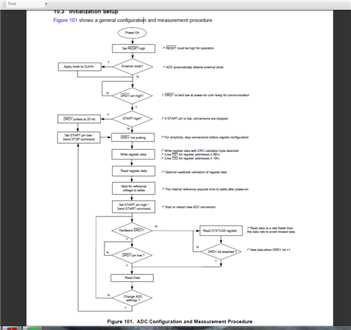
Part Number: ADS125H02

Hi,

I'm currently working on ADS125H02 interfacing with stm microcontroller. In this i'm using SPI for communication.

PIN connection :

HvVdd - +15 V

HvVss -  -15V

AVdd - 5V

DVdd - 3.3V

CapP n CapN - 1nF

RFout - grounded with 10uF

reset - float

START - assigned a pin as output from MCU for start pin (high n low condition)

SCK,DIN,DOUT,CS1,CS2 - connected with respective spi pins in MCU

DRDY - assigend a MCU gpio pin 

BYpass - connected to gnd with 1uF cap

CLKIN - grounded

AINCOM - Ground

AIN0 -  +5V 

AIN1 - ground (for single end adc conversion)

REF - using internal reference 2.5V
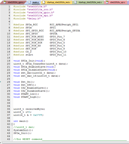
Below is the code  :-

int main()

{

//uint8_t dat;

SystemInit();

SPIx_Init();

//for RESET commond________________________________________________________

/*SPIx_EnableSlave();

SPIx_Transfer(0x06);//enable RESET commond

SPIx_Transfer(0x00);

SPIx_Transfer(0xA9); //accroding to crc value calculated

SPIx_Transfer(0x00);

SPIx_DisableSlave();*/

while(1)

{

//for START commond________________________________________________________

Set_On();

START_high();

/*SPIx_Transfer(0x08);//enable START commond

SPIx_Transfer(0x00);

SPIx_Transfer(0x7F); //accroding to crc value calculated

SPIx_Transfer(0x00);*/

START_low();


//UNLOCK_REGS_____________________________________________________________

SPIx_EnableSlave();

SPIx_Transfer(0xF5);//enable UNLOCK commond

SPIx_Transfer(0x00);

SPIx_Transfer(0x82); //accroding to crc value calculated

SPIx_Transfer(0x00);

SPIx_DisableSlave();

//reference___________________________________________________

SPIx_EnableSlave();

SPIx_Transfer(0x46);//enable internal reference commond

SPIx_Transfer(0x05);

SPIx_Transfer(0xE9); //accroding to crc value calculated

SPIx_Transfer(0x00);

SPIx_DisableSlave();

//for  MODE 4 WRITE________________________________________________________

//SPIx_EnableSlave();

CS2_EnableSlave();

//SPI_GPIO->BRR = CS_2;

SPIx_Transfer(0x50);//enable MODE4

SPIx_Transfer(0x34);//AIN0-COM , GAIN IS 0.5

SPIx_Transfer(0x57);//accroding to crc value calculated

SPIx_Transfer(0x00);

//SPIx_DisableSlave();

CS2_DisableSlave();

for(i=0;i<100;i++);


START_high();

Set_Off();


//for RDATA commond________________________________________________________

SPIx_EnableSlave();

SPIx_Transfer(0x12);//enable RDATA commond

SPIx_Transfer(0x00);

SPIx_Transfer(0xAA); //accroding to crc value calculated

SPIx_Transfer(0x00);

SPIx_Transfer(0x00);

SPIx_Transfer(0x00);

SPIx_Transfer(0x00);

SPIx_Transfer(0x00);

SPIx_Transfer(0x00);

SPIx_DisableSlave();


START_low();

}

}

While reading RDATA i'm receiving 20FFFF(1.2V)  for all voltage.

is there any changes i have to do?

please help me out with this issue.

Thanks in advance

  • Hi Sai,

    Can you double check your code and make sure that everything is accurate? I took a look at the MODE4 register command just to see what the gain was and noticed that you wrote the gain is 0.5 but your command (0x34) sets the gain to 1 V/V. This would send a 5V signal into the ADC using a 2.5V VREF, which wouldn't convert correctly. So please double check the code is correct and configures the ADC how you intended.

    Also, can you send a schematic of your system and the full register settings?

    -Bryan

  • following is my schematic

  • Hi Sai,

    Have you made any changes to the code? This issue could be a result of improper configuration, so I am hoping you can double check the code and make sure everything is how you intended.

    Can you also send me your full register settings? It would be helpful to double check this against a full register readback from the ADC itself to ensure that the correct register settings are being applied

    -Bryan

  • Hi Bryan,

    The above given image is my program,

    I done the program based on or with the help of Initialization_setup in the datasheet.

    the above given image is an Initialization setup.

    The output is not coming correctly.

    if i want to use Calibration steps please explain it, how to use it because after using that too ,i am not getting output.

    Thanking You,

    Sai.

  • Hi Sai,

    When you changed the gain from 1 to 0.5, did the output change? If you did not already run this test, can you?

    Also, how are you applying a signal to the ADC? You said there was 5V on AIN0, is this voltage from a precision source? Does the source voltage share a ground with the ADC PCB? Which ground is the voltage source connected to, AGND or DGND?

    The schematic shows two different ground symbols, do you have split ground planes on your PCB?

    -Bryan

  • Hi Bryan,

    yes it changed but not even close to the required output value for 5v it gave 2.5V only.

    I'm applying signal to AIN0 and grounded the AINCOM because i'm only using the single ended connection and also for this reason i grounded AIN1 too. 

    Yes from the precision source only and the ground is connected with AGND.

    Also i separately designed using this schematic in a bread board in that i gathered all the ground in a common point.

     I'm getting variation in output whenever i'm giving analog signal to AIN0.

    -Sai.

  • Hi Sai,

    In looking through your code I see that when you send the command to change the REF register, you are sending the write command (0x46) followed by the data (0x01) followed by the CRC (0x82). The first two commands are correct, however the correct CRC value for 0x4601 is 0xF5. So this likely means that the ADC is not implementing this register write and the internal reference is not being selected. Instead, the default settings use AVDD as the reference, which explains why your output is about 1/2 what you expect it to be.

    You can use our Excel-based calculator tool to help calculate the correct CRC values for the different commands: https://www.ti.com/lit/zip/sbac234. This is what I used to calculate the values mentioned above.

    -Bryan

  • No i'm using internal reference so my command should be 0x4610 for this CRC is 0x82 only. For this the ADS125 should use internal 2.5V .

    In my above program i gave it correctly.

  • Hi Sai,

    Yes you are correct, I had the data byte backward in my previous post.

    Have you confirmed that the ADC is actually writing the correct values to the registers? Can you read back the registers once they have been written and provide the results?

    Can you also provide a logic analyzer shot of the digital communication during the write transaction? Please include CS1, CS2, DOUT, DIN, and SCLK.

    You can also check the REFOUT pin to see if this is 2.5V.

    Please let me know the results of these tests.

    -Bryan