This thread has been locked.

If you have a related question, please click the "Ask a related question" button in the top right corner. The newly created question will be automatically linked to this question.

ADS7863A: sufficient timing information

Part Number: ADS7863A
Other Parts Discussed in Thread: ADS7863

Hello Team,

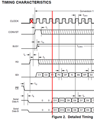
My customer is aware of the fact, that the ads7863a replaces the older version and they use the updated version in their design. Unfortunately they can't get sufficient timing information from the datasheet of the ads7863a.They can't seem to find any information on what edge the adc starts reading from sdi, or sends the first bit on sdoa/b.

Thanks in advance.

Regards,

Renan

  • Hello Renan,

    Thank you for posting their question.

    From Figure 2, it appears that the ADS7863A shifts data into the device on the CLOCK rising edge and latches SDI on the falling edge. The device shifts data out on Serial Data A and B on the CLOCK falling edge and the MCU should latch the data output on the CLOCK rising edge.

    The MSB on Serial Data A and B is shifted on the 4th CLOCK falling edge. 

    Regards,

    Ryan

  • Hello Ryan,

    Thank you for your response, however I still got some questions. 

    You state that the data is clocked out on the sdo ports beginning with the 4th falling edge.
    The datasheet says the following:
    Serial Data Output (SDOx)
    Converted data on the SDOx pins become valid with the third falling CLOCK edge after generating an RD pulse. The following sections explain the different modes of operation in detail.
    What does this mean?
    Can I assume, that the first bit on SDI is also latched on the 4th falling edge? Also what do you mean by the ADS7863A shifts data into the device on the rising edge and latches sdi on the falling edge? Does it shift in the data on the falling or the rising edge? 'Shift in the data' and 'latch the data' are the same to me.

    Regards,

    Renan

  • Hi Renan,

    What I meant by shifting the data is that the respective clock edge is changing the data to the next bit. On SDI, the bit change occurs with each clock rising edge, and on SDO, the bit change occurs on each clock falling edge. Data is read by the ADC on the clock falling edge and read by the host/MCU on the clock rising edge.

    Please refer to the timing diagram (Figure 2) in the device data sheet. The 3rd falling edge after the RD pulse aligns with the first bit transition on SDO, meaning SDO is now actively driven with valid data.

    Regards,

    Ryan

  • Hello Ryan,

    Thank you for your help.

    On which clock edge will the adc start to latch the data provided by the MCU/FPGA on SDI?
    Also 'On SDI, the bit change occurs on each clock rising edge.' The SDI signal is an input signal for the ADS7863, I understand that I change the data on the rising edge and the ADS7863 latches the data on the falling edge?

    Looking forward for your response.

    Regards,

    Renan

  • Yes - that is correct.

  • Hello Ryan,

    I apologize I didn't get your response clearly. Can you share which clock edge will the ADC starts to latch the data provided by the MCU/FPGA on SDI?

    Regards,


    Renan

  • Hi Renan  - the ADC begins to latch the SDI data on the clock falling edge labeled '1' in Figure 2. This is the first clock after the RD pulse.

    Regards,

    Ryan