Hi,
Good day.
Our customer is using the ADS8166 and they have the following question.
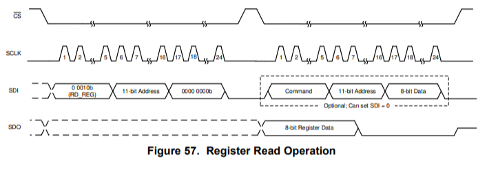
"With the register readout procedure described in the datasheet. I cannot readout any of the registers. I use a Raspberry Pi with spidev. The readout for register address 0x00 looks like this:
spi.xfer2([0b00010000;29;0x00]) #read command
data=spi.xfer2([0b00010000;29;0x00]) #should not matter what to send here according to datasheet
what i would expect would be the 8bit Register Data followed by two zero bytes.
What i get is two bytes (ADC value) followed by a zero byte.
However it is possible for me to change the ADC Channel with spi.xfer2([0b00001000,29,1])
I tested this with fixing one of the inputs to GND another one to a fixed voltage and getting data from both alternating between them. -> MOSI Line works and MISO as well
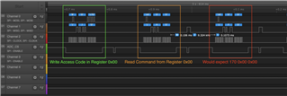
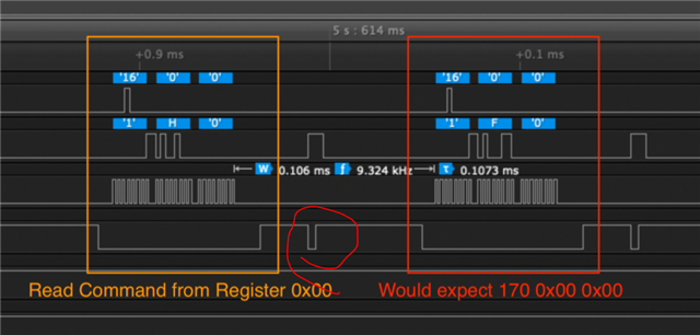
I hooked up a logic Analyzer to the system but it just verifys the data i get with the Rpi.
Because this write command worked I tried to blindly put the device in the debug mode. (Write the REG_ACCESS_BITS in the Reg Access Register and write 0x01 to Data_CNTL_Reg 0x10 to enable debug mode) but this failed as well and the ADC just gave me more 16 bit Data which was different from the debug value.
I checked the second SDO Line with the Logic Analyzer as well but it stays LOW all the time so is deactivated as expected.
Is there something I am missing to get Read Access to Registers?
Is there something missing to get Write Access to the Write Access Register or any other Register except for the Chan Id Register?
Do I need to stop the 16bit ADC Data Output before i can read Register Values?
If so how can I Stop the output? I already tried to powerdown the adc module but this failed as well.
Is there some special frequency I need to use? I tried 400000Hz 800000Hz 1600000Hz already
Do I need some special breaks/Read more bytes? Already tried burstread 6 bytes spi.xfer2([0b00010000,29,0x00,0b00010000,29,0x00]) Got [ADC_MSB;ADC_LSB; 0x00, 16,29,0]->just got back my message of the first three bytes after the usual frame."
We would appreciate your inputs on this matter. Thank you.
Regards,
Cedrick

-
Ask a related question
What is a related question?A related question is a question created from another question. When the related question is created, it will be automatically linked to the original question.