


I need to build an echo generator for testing an L band receiver composed by 8 channels for bandwidth range: 0÷400 MHz and n.2 channels for bandwidth range: 0÷500 MHz
The characteristic of the single channel tx is:
Bandwidth range: 0÷500 MHz
Center frequency output: 900MHz÷1200 MHz
PRF Configurable: 500 ÷ 7000 Hz
Pulse Width: 4 μs ÷ 100 μs
Tx duty cycles range: 2 ÷ 15 %
Rx duty cycles range: 10 ÷ 95 %
Power Output: 0 dBm ÷ -80 dBm
I would have other questions to ask.
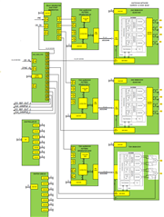
The system I would like to use consists of the following T.I. boards;
- 2 TSW 14J56 EVM boards and n.2 DAC 38J84 EVM boards for evm and n.1 LMK 04832 EVM board for the synchronous generation of n.8 RF chirps signals up to 2400 MHz for bandwidth range: 0÷400 MH.
The system is also composed of the following cards for the generation of n.2 RF chirps signals by modulators
- 1 TSW 14J56 EVM boards and n.1 TSW 38J84 EVM boards and n.1 LMK 04832 EVM board for the synchronous generation of n.2 RF chirps signals up to 2400 MHz with modulators for bandwidth range: 0÷500 MHz bandwidth.
In order to configure the i various individual parameters board, I will use your panel SW ( GUI) supplied by means the USB port.
In order to configure all the EVM Boards, I need to insert a USB hub and select one card at a time. Do you confirm to insert a USB Hub 3.0.
Is it possible to configure the N. 3 SW (GUI) related to the single EVM Boards with a single pc?
It is possible to modify the various internal registers of the EVM boards during the normal operational through SPI link, without having to load the single panel Sw ( GUI). If yes, how can I do………..
What are the connectors J24 ( DAC SPI) and J25 ( LMK SPI )located on the DAC 3XJ8X EVM board?
What are the connectors J9 ( DAC SPI) and J10 ( LMK SPI )located on the TSW 38J84 EVM board?
The system, after having loaded once the data from the PC into the DDR memory of the TSW cards, will have to generate the 8 echo signals from the DAC boards in loop mode.
The start echo generation signals will be synchronous with the appropriately delayed external PRI signal without having to reload the memory from USB.
At the end of the DDR memory unloading process , the echo generation signals must be initialized with the PRI signal without having to reload the memory from USB.
Thanks for collaboration
Stelvio
