This thread has been locked.

If you have a related question, please click the "Ask a related question" button in the top right corner. The newly created question will be automatically linked to this question.

ADS1248 Differential input question

Other Parts Discussed in Thread: ADS1248, ADS1148, OPA333, INA333, TPS60403

Hello everyone:

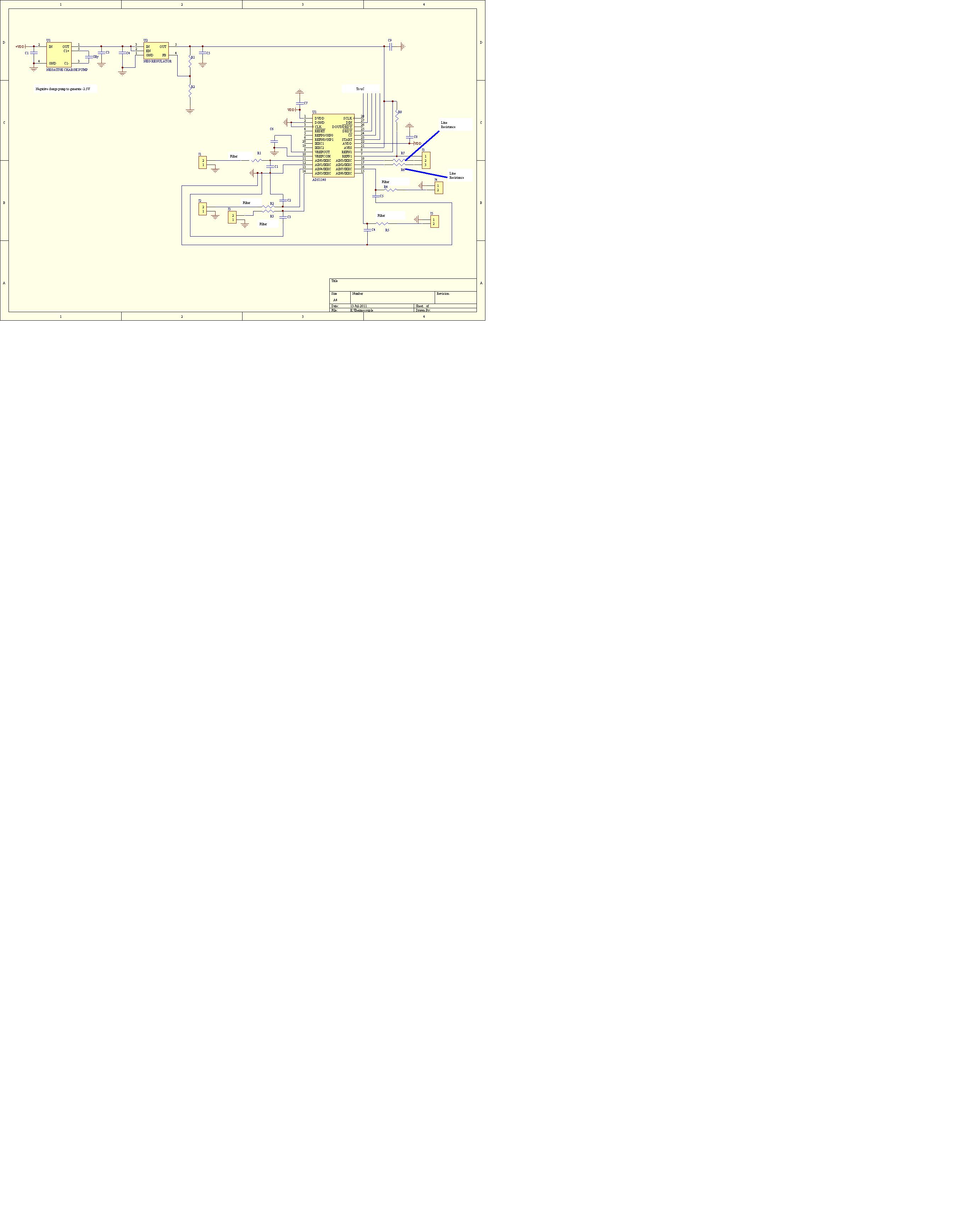
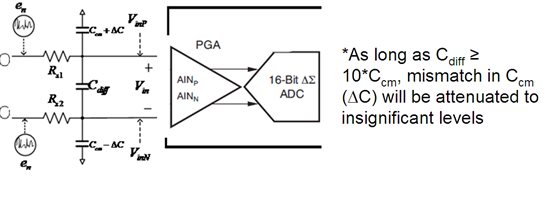
I am using a K type thermocouple to measure the temperature. Ther convertor is ADS1248. I use Differential input mode of ADS1248:connect the thermocouple to AIN0 and  AIN1. But the noise is very big. I tryed to use the VBIAS,and connect AIN0/AIN1 to GND,but it is not useful.

I want to know how to use the Differential mode and how to filter.

thanks!


best regards!

Youngchun

2011.03.11

  • Hi,


    In order to use the ADS1248 measuring thermocouples; the user could connect BIAS voltage generation for a set up using for ungrounded thermocouples.  The bias voltage is (AVDD + AVSS)/2 and should be connected to one of the terminals of the thermocouple.


    If a grounded thermocouple configuration is being implemented, the user will have to set up the ADS1248 using bi-polar supplies (typically +/-2.5V).  This is necessary to ensure the common-mode range requirements are met.  An equation is given on the datasheet that relates the differential voltage VIN, PGA gain and voltage supplies to calculate the common-mode input range on page 4.


    A simple RC low pass filter can be placed across the inputs of the converter to filter noise coming in from the lines of the thermocouple. 


    Other general suggestions to reduce noise are to use twisted pair extension wire to connect the thermocouple; and if possible isolate the thermocouple line away from noise sources.  Also, the user will need to ensure that the Reference has a decoupling capacitor; for example, if the internal reference is being used, the value of the capacitance should be 1uF to 47uF between VREFOUT and VREFCOM.  The voltage supplies AVDD and AVSS should also have appropriate decoupling capacitors close to the pin.

    Attached is application note SBAA180; page 5, Figure 5 shows an example with a thermocouple and filter.


    Please let me know if this helps or if you have any additional questions,


    Kind Regards,


    Luis

    2134.sbaa180[1].pdf

  • Hi Luis,

    Is it possible to have thermocouple connected as single-ended input to the ADS1148? I am planning to have 5 thermocouple along with a RTD connected to a single ADS1148 chip.

    Regards,

    Himanshu.V.Ajmera

  • Hello Himanshu,

    Yes, you may connect the thermocouples single ended.  One possible way to accomplish this is to connect one AINx input to GND and refer all thermocouples to GND and their positive terminal to other 5 inputs.  Since the thermocouples are referred to GND in single-ended fashion, you will need to bias the ADS1148 with bipolar supplies (+2.5V and -2.5V) in order to meet the common-mode voltage (VCM)  range requirements, where the allowed common mode voltage range is a function of the voltage supplies, differential signal and PGA gain:

    AVSS +0.1 + (Vdifferential)(GAIN)/2 < VCM < AVDD - 0.1 - (Vdifferential)(GAIN)/2

    where common mode voltage is defined as VCM= (AINP+AINN)/2 and Vdifferential=AINP-AINN.

    The PT100 will need two more additional inputs; with the Rbias resistor referred to AVSS.

    Regards,

    Luis


  • Hi Luis,

    Thanx for the earlier reply. We won't be able to provide bipolar voltage in my project so can you suggest some solution for that?

    I was thinking for DC/DC converter but not sure whether that would work for me? or do then do I need to go for differetial input?

    Thanx,

    Himanshu.V.Ajmera

  • Hi Himanchu,

    There are two possible solutions that I can think of.  If the thermocouples are not required to be grounded, one solution is to connect the thermocouples to the ADS1148 using an Instrumentation amplifier.  Below may be a possible solution using the INA333 and OPA333 to convert the differential signal coming out of the thermocouples into single-ended signals referred to the middle of the supplies.


    Another possible option for the ADS1148 16 bit converter is to generate your +/-2.5 Supply and leave the thermocouples referred to GND.  For example, the positive supply may be generated using a power regulator such as the TPS73001 and the negative supply with a combination of the TPS60403 negative charge pump voltage inverter and TPS72301 negative output linear regulator.   The power management forum engineers have expertise on this note and may be able to provide detailed support or may offer other options.  Please see below.

    Thank you and Regards,

    Luis


  • Hi Luis,

    Thanx a lot for your replies.

    Regards,

    Himanshu.V.Ajmera

  • Hi Luis,

    Can you please verify my schematic? I have attached and I wasn't too sure so thought to check with you before proceeding ahead.

    Thanx,

    Himanshu.V.Ajmera

  • Hi Himanshu,

    I have some suggestions:

    1)  VREFCOM pin needs to be grounded.

    2)  VREFOUT requires a coupling capacitor in the range from 0.1uF to 47uF for stability. The ADS1248EVM uses a 10uFcapacitor.

    3) If you are using bipolar supplies +/-2.5V; and measuring an RTD,  you probably need to refer RBIAS (R8) to the negative supply AVSS, and connect VREFN to the negative side of RBIAS (R8) (AVSS side) and VREFP to the positive side RBIAS (R8).   

    3) AVSS, AVDD, DVDD require coupling capacitors to be placed close to the ADS1148 device. The ADS1148EVM uses 10uF capacitors.

    4)  When designing the switching supply circuit, please consider that the maximum voltage for the ADS1148 is (AVDD - AVSS) < 5.25V.  If you are using +VDD=5V to generate the negative supply (AVSS); VDD will have to go through a voltage regulator to be set at +2.5V before connecting to AVDD.   

    5) When laying out the board; place the low-pass filter capacitors C1 - C5 close to the inputs of the device.  Use COG capacitors if possible.

    6) SPI connections are missing; but I am assuming this is work in progress. 

    It may be helpful to refer to the ADS1148EVM schematic for component values suggestions and to check how the general layout flow was completed since the device grounding and board layout is also critical in order to ensure that the device works properly.   If you like,  you could also submit a post on the power management forum for suggestions on the switching power supply components.   I will be happy to go through to the schematic again when completed.  Please find the ADS1147EVM link below.

    Thank you and Regards,

    Luis

    http://focus.ti.com/docs/toolsw/folders/print/ads1148evm-pdk.html

  • Hi Luis,

    Thanx for verifying my schematic and providing me the necessary feedback.As per your suggestion, I have made following changes:

    1)VREFCOM is being grounded.

    2)VREFOUT is connected to a coupling capacitor.

    3)RBIAS (R8) for RTD has been connected to AVSS via VREFP and VREFN i.e. +ve side of RBIAS is connected to VREFP and -ve side is cnonected to VREFN biased through AVSS .

    4)Coupling capacitor has been added to different supply-AVSS, AVDD and DVDD.

    5) Different SPI connections are added.

    I have attached the modified schematics and would ask you to verify the same. I am planning to put the same in power management forum for them to review and if they could suggest me with a better idea for negative supply.

    Thanx,

    Himanshu.V.Ajmera


  • Hi Himanshu,

    Thank you for the updated schematic. 

    1) The RESET pin needs a pull up resistor to DVDD.  If the processor has a free GPIO; you could connect this pin to the micro-controller to be able to control.  Also START,CS  need pull up resistors.

    Another suggestion is to add foot prints for an 'optional' low pass filter on the RTD input (AIN3,AIN2) for flexibility; if you decide not to use it, you can always populate with 0 Ohm resistors and not populate the capacitors. Note: The application note SBAA180 in general recommends no filtering to be added to the Input or reference signal paths when performing RTD ratiometric measurements using the IDAC's.  This is certainly true in most circumstances; but it is also depends on the environment.  In some circumstances, depending on the environment,  a light low-pass filter could be useful.

     Please let me know when you finish adding the components to the Switch supply and the voltage regulator to the AVDD supply.

    Thanks and Regards,

    Luis


  • Hi Luis,

    Sorry, I was not in the office yesterday so couldn't reply u.I have some doubts. U mention about flexibility after adding low-pass filter, I didn't get the idea of flexibility?

    If not using the low-pass filter, we can populate with 0 ohms resistors, what I get the idea is to add these resistance in series with the line resistance. Is this right?

    Can u give me some examples wherein such low pass filter has to be used? I have certain measurement which is to be done using RTD, so I can make such changes even to that circuit.

    What is the value of ΔC?

    Thanx for the earlier reply.

    Thanx,

    Himanshu.V.Ajmera

  • Hi Himanshu,

    Reading through the application note SBAA180, the application note provides optimal examples on how to configure and connect  the RTD's with the ADS1248.  It is recommended that when the IDAC current is used to excite the RTD; that this IDAC current is also used to produce a voltage accross RBIAS to generate the voltage reference used for the conversion.  This creates a ratiometric measurement where the drift and noise of the excitation is seen both at the reference path and the signal path.  Since this noise and drift is seen by both the signal path and the reference path they tend to cancel.  Applying a heavy filter to the RTD signal path could create a mismatch of the noise/drift that is seen at the RTD signal path and the reference path; and the user will not have an effective ratiometric measurement . However, depending on the users particular situation, and the specific nature of the noise in the users environment, in some cases may be beneficial to add a light low-pass filter on the RTD channel. For example, some customers choose to use a EMI or RF filter at the RTD channel; the corner frequency of the filter for EMI/RF filter is much higher than the noise components of the excitation current.  The decision to use a low-pass filter will depend on the noise environment on the engineers particular application and the engineer's decision should be based on their noise environment and their experimental results. 

    The application note refers to the parasitic line resistances of the connections between the remote RTD and the ADS1248.  The two wire is the simplest  method to connect the RTD; but the line resistances may cause errors when the RTD is placed far from the ADS1248 device. The three-wire  configuration greatly reduces the errors due to the parasitic line impedances.  If you choose to use the three-wire configuration with hardware compensation, you could choose to add a compensation resistor in the second arm of the RTD.  The RCOMP is a precision, very low temperature coefficient resistor chosen so that is equal to the RTD resistance in the middle of temperature range.  This provides the advantage of providing a measurement that is centered around 0V differential and may allow to use more gain on the PGA. The four-wire configuration provides the highest level of accuracy since it isolates the excitation path of the RTD to the sensing path.  Please refer to the SBAA180 application note link below.

    The ΔC in the discussion of the RC differential filter below is dependent on the mistmatch of the capacitors (Ccm) used on the filters on the two channels where the differential measurement is taking place.   To minimize the effects of the capacitor's  mistmatch, it is recommended to use a filter with a capacitor across the inputs (Cdiff) that is 10 times larger than the Ccm capacitors chosen.  The values of the Cdiff, Ccm depend on the corner frequency that is desired.  Please find the power point slide  "lowpassdiff.ppt" atttached for a generic differential filter below.

    Regards,

    Luis

    http://focus.ti.com/general/docs/litabsmultiplefilelist.tsp?literatureNumber=sbaa180

     2656.lowpassdiff.ppt


  • Hi Luis,

    That really helped me alot and cleared many doubts of mine. Thank you so much.

    Thanx,

    Himanshu.V.Ajmera

  • Hi Luis,

    I have finished the schematic and have cleared most of my doubts now. I have even added the low pass filter to my other project, which uses RTD for temperature measurement.

    I have added pullup resistor for RESET pin and for START and CS pins. I hope this time to get a clearance for my schematic.

    Thanx,

    Himanshu.V.Ajmera

    4718.Schematic.pdf

  • Hello Himanshu,

    On the ADC side, the schematic seems ok, as the components are connected properly; (the only exception R4 shows shorted).

    On the switch voltage supply circuit,  please consider that the maximum voltage for the ADS1148 is (AVDD - AVSS) < 5.25V.  If you are using +VDD=5V or VDD=3.0V to generate the bipolar +/-2.5V supplies; VDD will have to go through a voltage regulator to set AVDD to +2.5V in order to not exceed the maximum supply voltage for the ADS1148.  The Power management forum may be able to provide support on that end.

     
    Thanks and Regards,

    Luis

  • Hi Luis,

    The shorting at R4 was a small mistake.

    I am definitely going to use a voltage regulator and remembered that after I had attach the schematic here. I have already got my schematic checked from the power management forum regarding the bipolar supply

    Thanx for all the replies.

    Thanx,

    Himanshu.V.Ajmera.