This thread has been locked.

If you have a related question, please click the "Ask a related question" button in the top right corner. The newly created question will be automatically linked to this question.

DAC38RF82EVM: No output is observed across DAC.

Part Number: DAC38RF82EVM
Other Parts Discussed in Thread: DAC39J84, TSW14J57EVM

Hi,

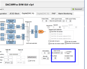
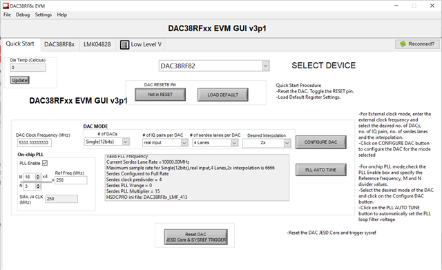
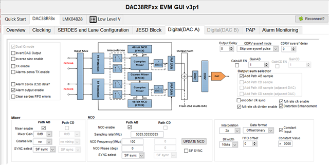
I have configured the DAC38RF82EVM using GUI. we are using CMODE3, with PLL frequency =250MHz.

# of DACs = Single (12bits)

# of IQ pairs per DAC = real input

# of serdes lane per DAC = 4 lanes

Desired Interpolation= X2

GUI Quick Configurations: 

"Valid PLL Frequency
Current Serdes Lane Rate =10000.00MHz
Maximum sample rate for Single(12bits),real input,4 Lanes,2x interpolation is 6666
Serdes Configured to Full Rate
Serdes clock predivider = 4
Serdes PLL Vrange = 0
Serdes PLL Multiplier = 15
HSDCPRO ini file: DAC38RF8x_LMF_413"

We have also observed that PLL LF Voltage = 4.

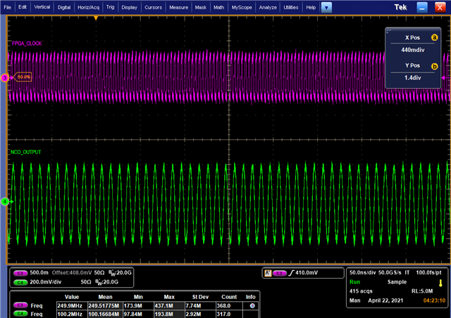
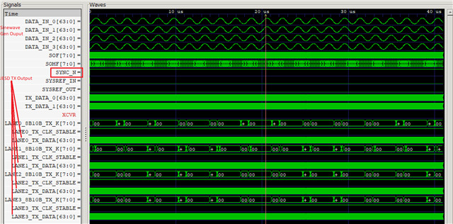
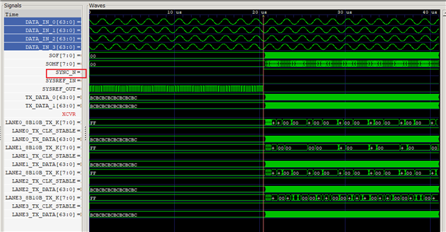
We have observed that, we have correctly received SYNC0B (High) from JESD204B RX of DAC38RF82EVM. 

I have attached PPT of GUI configurations.

Are we Configuring DAC38RF82EVM correctly. Please check and let us know, if you find anything wrong.

Thanks,

Imran

No DAC Output.pptx

  • Hi Imran,

    Looks fine to me on the initial look. Please advise the following:

    1. you have started out with using the automated script generation within the GUI, and then added the PLL configuration later.

    2. you are using the TSW14J56 EVM for this setup. If not, please advise if you have a way to use either Signal Tap or ChipScope to monitor the transition of the SYNC signal vs. K28.5 (CGS) and ILAS code transition.

    3. There should be a "resync" button at the front GUI menu to resync DAC JESD core. Please try this to force the DAC JESD204 block to be reset and re-initiate the hand-shake

    4. There should be constant tone pattern by enabling the constant input, set constant value to be 0x3FFF for instance (with default 2's complement format). You should observe a tone at the NCO output. Please try this and report back. This should verify the DAC itself is configured correctly. 

  • Imran,

    With the settings you have chosen, you cannot generate the proper SYSREF frequency. You must change something. Attached is an example that will work for you.

    Regards,

    Jim

    DAC38RF82_6400M_PLL_300M_ref_413.pptx

  • Hi Kang Hsia,

    Thanks for the reply. Please see my inline response. 

    1. you have started out with using the automated script generation within the GUI, and then added the PLL configuration later.

      [Imran] : We are following below steps:

          1. DAC RESETB

          2. LOAD DEFAULT.

          3. Then we are changing other parameter as per our requirements.

    2. you are using the TSW14J56 EVM for this setup. If not, please advise if you have a way to use either Signal Tap or ChipScope to monitor the transition of the SYNC signal vs. K28.5 (CGS) and ILAS code transition.

    [Imran] : We are not using TSW14J56EVM, We are using FPGA board. We have way to monitor internal signal ("Identify- tool from             Synopsys") like Signal Tap or ChipScope. We have observed that SYNC signal gone high, But need to check on trigger for K28.5 (CGS) and ILAS Code transition. we will try to capture those details and report you back.

    3. There should be a "resync" button at the front GUI menu to resync DAC JESD core. Please try this to force the DAC JESD204 block to be reset and re-initiate the hand-shake

    [Imran] : We didn't see any button with name "resync" at the front menu.

    4. There should be constant tone pattern by enabling the constant input, set constant value to be 0x3FFF for instance (with default 2's complement format). You should observe a tone at the NCO output. Please try this and report back. This should verify the DAC itself is configured correctly.

    [Imran] : we will try this step and let you know the observations. We are using Oscilloscope to observe output on DAC output SMA. Does this NCO output is DAC output SMA or something else?.

    Thanks,

    Imran

  • Hi Jim,

    Thanks for the reply.

    We are using the same GUI settings as mentioned in your PPT with just small difference.

    In our PPT,  LMK04828--> CLKout0 and 1-->DCLK Source--> Divider + DCC + HS

    In your PPT, LMK04828--> CLKout0 and 1-->DCLK Source--> Bypass.

    We will try above DCLK Source as "Bypass" for CLKout0 and 1 and let know the observations.

    Thanks,

    Imran

  • Hi Kang Hsia,

    we have tried enabling constant input and have set constant value to 0x3FFF, but we are not seeing any output across DAC output pin.

    we have monitor the SYNC~ signal in FPGA and observed that correct CGS and ILAS code transitions. after monitoring internal signal, it seems that JESD204B TX + XCVR is working correctly. Please see the attached PPT for monitored internal signal waveform with SYNC~ triggered. please let us know if anything else need to be done.

    Thanks,

    Imran

    InstrumentedInternalSYNC~Signal.pptx

  • Hi Kang Hsia,

    Please note that, we are not using CAR_SYSREF_P/M signal. 

  • Imran,

    How is the FPGA getting SYSREF if you are not using CAR_SYSREF? This DAC only supports subclass 1 mode and the FPGA must get a proper SYSREF signal.

    Regards,

    Jim

  • Hi Jim,

    In previous project, we have used DAC39J84, where we have supplied SYSREF signal to DAC from JESD204B TX IP (from FPGA) via FMC_SYSREF pin.  but on DAC38RF82EVM, we did not see this pin (FMC_SYSREF) in schematics. So we did not connect to JESD204B TX IP (to FPGA). Sorry for the confusions.

    I will try to use the CAR_SYSREF signal as input to FPGA (JESD204BTX IP) and let you know the result.

    Thanks,

    Imran 

  • Hi Jim,

    I tried using the CAR_SYSREF signal with our JESD204B TX IP SYSREF input signals, but still not getting output across DAC output SMA.

    Is there any way, we can quick test DAC38RF82EVM functionality without FPGA? or Do we have any other internal signal pattern testing option available on DAC38RF82EVM?.

    I have attached the design block diagram and internal debug signal PPT. 

    Please look at it and let me know your suggestions.

    Thanks,

    Imran

    Design Block diagram and internal signal debug_1.pptx

  • Imran,

    I do not see a device clock going to the FPGA in your block diagram. Where is this coming from and at what frequency? Do you get a DAC output when using the NCO only mode? After you pass this test, then you can focus on the JESD link. If the NCO can provide an output, when attempting to run with JESD data from the FPGA, if CGS and ILA pass, what errors are reported by the DAC? Can your FPGA run with serdes rates at 12Gbps? I am assuming all of your clock frequencies and DAC settings are now per the power point slide I sent. Is this still correct?

    Regards,

    Jim  

  • Hi Jim,

    Sorry for the inconvenience.

    Device clock is coming from DAC38RF82EVM. it is 250MHz. I am unable to get DAC output with constant input enable with 0X3FFF constant data. 

    I don't know how to perform NCO mode only test on setup with GUI. Can you please share GUI setting to enable NCO mode only?. I like to perform NCO mode only test.

    Our FPGA can runs up to 12.5Gbps, but we are only configuring at 10Gbps.

    All GUI settings and DAC settings are as per your slide only, except SerDes Data rate is 10G and PLL clock is 250MHz. All other settings are same.

    Thanks,

    Imran

  • NCO only mode instructions attached.

    2234.DAC38RF82_NCO_Only_Test.pptx

  • You cannot use my settings with a 250MHz PLL clock. This would set the serdes to 13.33Gbps. You must have changed something else.

    What is the M and N PLL settings? I had 16 and 3. What is else is different?

    Jim 

  • Hi Jim,

    Ref Freq = 250MHz, M=16 and N=3.

    Please see the attached Image of "Quick Start".

    Thanks,

    Imran

  • Hi Jim,

    Now i am able to get the NCO output on J7 SMA (DAC output pin)

    GUI setting: NCO Frequency is 100MHz.

    Thanks,

    Imran

  • Imran,

    I was using single DAC instead of 12-bit DAC mode, thus I came up with the wrong serdes rate. I setup my system to use your latest settings and got a valid output using our TSW14J57EVM pattern generator. I saved the register settings and they are attached.

    Regards,

    Jim

    DAC38RF82_Fs_5333M_413_250M_PLL.cfg 

  • Hi Jim,

    I tried using above .cfg file. but still not getting any output on J7 SMA. I tried checking the Alarm monitoring and observed the below errors:

    "PLL in the Rincewind1 block goes out of lock. A false alarm is generated at startup when the PLL is locking. User will have to reset this bit after start to monitor accurately.

    "DAC A, Lane 0 write_error : High if write request and FIFO is full (NOTE: only released when JESD block is initialize with mem_init_state)"

    "DAC A, Lane 0 read_error : High if read request with empty FIFO (NOTE: only released when JESD block is initialize with mem_init_state)"

    "DAC A, Lane 1 write_error : High if write request and FIFO is full (NOTE: only released when JESD block is initialize with mem_init_state)"

    "DAC A, Lane 1 read_error : High if read request with empty FIFO (NOTE: only released when JESD block is initialize with mem_init_state)"

    "DAC A, Lane 2 write_error : High if write request and FIFO is full (NOTE: only released when JESD block is initialize with mem_init_state)"

    "DAC A, Lane 2 read_error : High if read request with empty FIFO (NOTE: only released when JESD block is initialize with mem_init_state)"

    "DAC A, Lane 3 write_error : High if write request and FIFO is full (NOTE: only released when JESD block is initialize with mem_init_state)"

    "DAC A, Lane 3 read_error : High if read request with empty FIFO (NOTE: only released when JESD block is initialize with mem_init_state)"

    please let me know are these errors are relevant?

    Thanks,

    Imran

  • Imran,

    Please follow the steps in the start-up sequence shown in section 9.1.1 of the data sheet. Make sure to sync the CDRV and JESD blocks after all registers are written and the FPGA is sending the K28.5 characters. The last write to the DAC should be to take the JESD core out of reset. 

    If this does not help, double check the FPGA settings and clocks as to me appears the CGS is not getting established. What is the status of the SYNC signal?

    Regards,

    Jim 

  • Hi Jim,

    We will try to follow the start-up sequence mention in datasheet.

    In FPGA, we are receiving signal SYNC_N as high after K28.5 characters. Please see the attached.

    we have tried to trigger the SYNC_N signal, please see the attached images.

    Thanks,

    Imran 

  • Imran,

    What is the status of TXENABLE? If low, the DAC will not have an output. Before reading any alarms, you must first write a "0" to clear them.

    How did your DAC register settings compare to the ones I sent?

    Regards,

    Jim

  • Hi Jim,

    TXENABLE pin is high on DAC EVM ( JP2 jumper is shunt pin1-2- Enable DAC output).

    We tried clearing alarm register, before reading them and We are not getting any alarm errors on Lane0-Lane3. 

                 "lane 6 loss of signal

                  lane 5 loss of signal

                  lane 4 loss of signal

                  PLL in the Rincewind1 block goes out of lock. A false alarm is generated at startup when the PLL is locking. User will have to reset this                bit after start to monitor accurately."

    We have also compared our DAC register settings with your DAC register settings sent earlier for same configuration.

    Observed only few registers are different:

    LMK register --> 0x13B = 0x3C (0x0F in your .cfg file)  

    DAC register --> 0x433 = 0x083C (0x053C in your .cfg file).

    Thanks,

    Imran

  • Imran,

    What FPGA platform are you using? Since you are only using 4 lanes, it it normal to see errors on the 4 unused lanes as you are reporting. In 4 lane mode, only one Rincewind PLL should be locked. In your case, this would be Rincewind0.

    Please use the same setting as our config for LMK address 0x13B. This is the SYSREF divider. Are you clicking on the "Reset DAC JESD core and Sysref Trigger" button on the DAC GUI after the FPGA is setup? 

    Regards,

    Jim

  • Hi Jim,

    We are using PolarFire FPGA.

    I have tried to change the value of LMK address 0x13B to 0x0F via Low Level Vi --> Write register.

    and also I have tried to change SYSREF divider in GUI (LMK--> SYSREF and SYNC--> SYSREF divider value to 15). but still no output across DAC output SMA.

    Yes, We are clicking on the "Reset DAC JESD core and Sysref Trigger" button on the DAC GUI after the FPGA is setup.

    Thanks,

    Imran

  • Imran,

    Is your RBD value less than your K value? 

    Can you try a mode that does not use the DAC PLL and maybe only 1 or 2 lanes?

    Not sure what else to tell you. Do you have a TSW14J56EVM to verify the functionality of the DAC38RF82EVM? If you do not have the TSW board, you can send me the DAC38RF82EVM you have and I will send you a tested board in return.

    Regards,

    Jim

  • Hi Jim,

    I am not sure about RBD, but it might be equal to K.

    I will try to use test mode without DAC PLL with 1 or 2 lane design.

    I need to check, we might have TSW14J56 board.  We have one more DAC38RF82EVM card, I can use that with same setup and test it out.

    Thanks,

    Imran