This thread has been locked.

If you have a related question, please click the "Ask a related question" button in the top right corner. The newly created question will be automatically linked to this question.

ADC124S051: Crosstalk between multiplexed channel conversions

Part Number: ADC124S051

Hello,

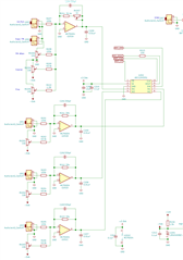
I'm using the ADC124S051 connected to an FPGA and running at the maximum 8MHz clock rate to convert 4 different signal sources in a continuous round-robin cycle. I am seeing noticeable crosstalk between the multiplexed inputs, where the results of the immediately prior conversion are affecting the current conversion. I have tried an number of approaches to fix this:

1) Slowing down the sample rate from 500kSPS to 375kSPS - didn't help.

2) Stalling the SPI clock during the sample acquisition period by several microseconds to extend the settling time - didn't help.

3) Introducing long periods of /CS de-asserted (high) to separate the conversions - didn't help.

4) doing two successive conversions per channel and only using the 2nd result - the 2nd result is still contaminated.

The only thing I've found that prevents crosstalk between the channels is to not change the mux setting - only convert one input channel continuously. That prevents crosstalk but of course doesn't allow me to sample all four channels as my system requires.

I am driving the ADC inputs directly with low impedance op-amp outputs, and I also have 0.01uF caps near the pins to serve as charge reservoirs for the sampling process. I have confirmed with bench DMM measurements that the analog voltages into the ADC are not affecting each other externally.

Are there any suggestions for how I might solve this problem?

Thanks,

Eric

  • Hello,

    All the actions you have taken would be my first line of defense when seeing cross talk issues. 

    But you say that if you sample one channel continuously, without muxing, eventually you get the expected results. I would then suggest adding a low series resistance between the cap and the op amp, ~200omh, and decreasing the 0.01uF cap to 680pF. 

    Also, would you share your schematic for review? Including the input drive circuit. 

    My next suggestion would be to evaluate the PCB, is the layout causing any issues. 

    Regards

    Cynthia

  • Hi - thanks for the suggestions. I'll try playing around with the cap values to see if it makes any difference in the behavior. Putting resistors in between the op amps and ADC will be a challenge on this PCB but I'll give it a try. 

    Here's a portion of the schematic showing the ADC and drivers:

  • Hello Eric, 

    From your schematic, I would strongly suggest adding a series resistor to the output of the op amp. Op amp cannot drive a fully capacitive load; you currently have the op amp driving a single cap and then the switch capacitor circuit of the ADC. 

    I believe once the resistor is added, and optimizing the capacitor value, you will see correct measruements. 

  • I agree that the 0.01uf cap without the series resistor is likely pushing the op-amp into dangerous territory - the datasheet for the part I used suggests that anything more than 100pf or so requires the a few hundred ohms. My PCB layout doesn't allow me to easily add the resistor, so as an experiment I tried simply removing the capacitors. This eliminated the crosstalk completely and doesn't seem to have made the system more sensitive to other kinds of noise, so the issue is resolved.

    Someday when I have time I may explore if the R+C approach also works - I'm curious what the exact mechanism of the error is. For now however this seems to indicate that the capacitor on the that node is not just unnecessary, but actually harmful.

    Thanks for the help.