This thread has been locked.

If you have a related question, please click the "Ask a related question" button in the top right corner. The newly created question will be automatically linked to this question.

ADS7841: ADS7841E

Part Number: ADS7841
Other Parts Discussed in Thread: TMS320F28379D,

Dear  sir/madam,

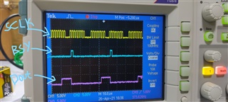
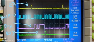
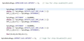
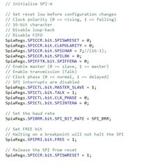
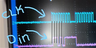
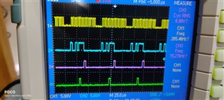
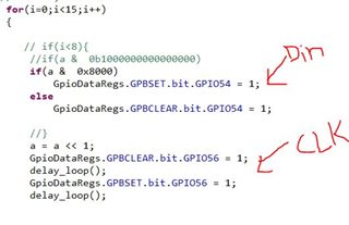
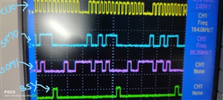
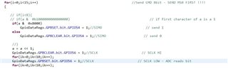
im trying to interface tms320f28379d with ads7841 via spi but getting random junk with or w/o connecting voltage to selected channel through control byte .

check screenshots and correct me if
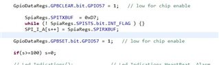
 im wrong.

  • Hello, 

    the best way to debug code is through a visual check of the communication. Connect probes to the digital bus to verify that the code is doing what is expected. 

    To debug, I suggest using a known DC input at the analog input, this will allow to compare the output measurement to the expected output. 

    you can then use the scope shot and compare to the timing diagrams in the datasheet to confirm al timing requirements are met. 

  • These are the scope images when i connect to spi lines with spichar = 7;

  • Thank you

    Can you can a scope shot with CS, SCLK, and DIN together. 

    From what I am gathering here, you are sending a control bite, right after another. A new control byte can only start every 15th clock cycle in 12-bit conversion mode or every 11th clock cycle in 8-bit conversion mode.

    your BUSY and DOUT also look wrong. BUSY should go high after a valid control byte, from the image, it seems busy is not doing this.  Also, it seems that you have DOUT data before BUSY goes does. this is a big indicator that something is wrong. BUSY goes high after the control byte, not until after BUSY goes back down does DOUT data should be outputted. 

    I believe you are communicating to the part incorrectly. Please look over the control byte, clock and timing requirements. 

    Regards

    Cynthia

  • Hai Cynthia,

    Could to send me the steps to do for interfacing tms320f28379d with ads7841 as i cant get output  after trying all combinations from my side.

  • From your images, it looks like you are taking a single ended measurement of channel 1. you are also using 12 bit conversion mode. is this what you are expecting to do?

  • Hi cynthia,

    What you said is exactly what i'm trying to do.I also tried 15 clock cycles operation also by using bit operations on data and clock pins eventhough result was same. Mode pin tied to ground and busy pin was kept floating and forstly trying to see result in scope as per given graphs in datasheet but something is wrong.

  • Taking a closer look at the scope shot, it looks like the DIN is not synced with the clock. 

    The DIN bit should change at the falling SCLK edge and be stable at the rising edge of SCLK to be read by the device. 

    The start bit in DIN should be high before the first rising SCLK as well. 

    Regards

    Cynthia

  • Im using 15 clock cycles and command byte was 0x97 using channel 0(0v was given as input),mode bit was low (12bits conversion),single ended and always power on ,CS pin was low always.But how im getting high on Dout when 0v connected.Is anything wrong,im using toggling operation on pins for CLK,CS,DIN(writing),DOUT(reading) not spi.

  • I believe it is working well. You have 0V connected, and you are only measuring 0x01, which is only 1 LSB above your expected output. This is within the performance of the device.  

    If you want to learn more about simple calibration methods, here is a short document that includes a 2 point calibration method starting on page 5 in "Reducing Effects of external RC filter"

    Regards

    Cynthia

  • i've connected 3.2 v to channel0 and vref and vcc for ads7841 is connected to 3V the expected output is 4096 from SOMI pin but data was as screenshot above .please verify SOMI whether it was alright.

  • From your screenshot, I gather that SDO measured 621, which with a 3V ref translates to about 455 mV. What were the other channels connected to? Can you make sure the other channels are connected to known DC inputs that are different from CH0. Example, Ch0 = 3.2V, CH1=Ch2=Ch3=1V

    I would now suggest looking at your hardware, making sure that the inputs are being driven correctly. 

    Also, what is the frequency of your clock? From the screenshot, I believe it is 164kHz. If this is correct, then you will need to decrease this to a maximum of 125kHz.

    Regards

    Cynthia