This thread has been locked.

If you have a related question, please click the "Ask a related question" button in the top right corner. The newly created question will be automatically linked to this question.

ADS1261: SPI MISO is only echoing MOSI line data

Part Number: ADS1261

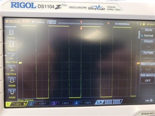
Currently trying to set up communication from my STM32L471ZETx to the ADS1261 to read load cell data. I believe I have the code structured correctly from following the example code ( https://www.ti.com/product/ADS1261#design-development##software-development) and something configured poorly since I'm receiving a response to commands sent to the ADC but the responses are only echoing the data I send (every data byte, not just the initial echo byte that should be expected). Is there anything I should be looking for or a resource I can use to troubleshoot? I've attached the setup and actual communication of the SPI, if there's anything else I can attach, let me know. Thanks in advance!

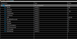
static void MX_SPI3_Init(void)
{

  /* USER CODE BEGIN SPI3_Init 0 */

  /* USER CODE END SPI3_Init 0 */

  /* USER CODE BEGIN SPI3_Init 1 */

  /* USER CODE END SPI3_Init 1 */
  /* SPI3 parameter configuration*/
  hspi3.Instance = SPI3;
  hspi3.Init.Mode = SPI_MODE_MASTER;
  hspi3.Init.Direction = SPI_DIRECTION_2LINES;
  hspi3.Init.DataSize = SPI_DATASIZE_8BIT;
  hspi3.Init.CLKPolarity = SPI_POLARITY_LOW;
  hspi3.Init.CLKPhase = SPI_PHASE_2EDGE;
  hspi3.Init.NSS = SPI_NSS_HARD_OUTPUT;
  hspi3.Init.BaudRatePrescaler = SPI_BAUDRATEPRESCALER_8;
  hspi3.Init.FirstBit = SPI_FIRSTBIT_MSB;
  hspi3.Init.TIMode = SPI_TIMODE_DISABLE;
  hspi3.Init.CRCCalculation = SPI_CRCCALCULATION_DISABLE;
  hspi3.Init.CRCPolynomial = 7;
  hspi3.Init.CRCLength = SPI_CRC_LENGTH_DATASIZE;
  hspi3.Init.NSSPMode = SPI_NSS_PULSE_DISABLE;
  if (HAL_SPI_Init(&hspi3) != HAL_OK)
  {
    Error_Handler();
  }
  /* USER CODE BEGIN SPI3_Init 2 */

  /* USER CODE END SPI3_Init 2 */

}

void SPITask(void *arguments) {
    uint8_t transmission_buf[6] = { 0x12, 0x03, 0x00, 0x00, 0x00, 0x00};
    uint8_t start_conversion_buf[2] = { 0x08 ,0x03 };
    uint8_t reset_buf[2] = { 0x06,0x03 };
    uint8_t receive_buf[6] = { 0x00,0x00,0x00,0x00,0x00,0x00 };
    uint8_t id_buf[6] = { 0x20,0x00,0x00 ,0x00,0x00,0x00 }; //read id register

    HAL_GPIO_WritePin(GPIOB, ADC1_nPWDN_Pin, GPIO_PIN_SET); //pwdn pin is high before conversions
    HAL_GPIO_WritePin(GPIOB, ADC1_nRESET_Pin, GPIO_PIN_SET); //reset pin is high before conversions
    HAL_GPIO_WritePin(GPIOB, ADC1_START_Pin, GPIO_PIN_SET); //start pin is high before conversions
    //poll for the drdy bit
    while(HAL_GPIO_ReadPin(GPIOB,ADC1_nDRDY_Pin) == 1);
    for (;;) {
        HAL_SPI_Init(&hspi3);
        HAL_SPI_TransmitReceive(&hspi3, (uint8_t*)id_buf,(uint8_t*) receive_buf, 6, 100);
        HAL_SPI_DeInit(&hspi3);
    }
} 

  • Hi Ryan,

    Do you have logic analyzer data to show the SPI transactions on all digital lines? That would be helpful to understand what is going on here.

    I use a Saleae logic analyzer so if you use the same device you can just send the data file and I can open it on my end, instead of sending still images.

    -Bryan

  • We just got our oscilloscope/logic analyzer in last week but I'm having some issues connecting it to our board. We got the DS1074Z Plus with RPL1116 digital probe addon (https://www.rigolcanada.com/products/digital-oscilloscopes/1000z/). We're completely new to embedded development so there may be something we're missing on the board but there's no way to clip our logic analyzer to the chip. Is soldering a short wire onto the pins (as seen in this article https://articles.saleae.com/logic-analyzers/logic-analyzer-tutorial-probe-setup) the best way to be able to connect the analyzer? 

  • Hi Ryan,

    I guess the answer is "whatever works". Ideally there should be header pins on the digital lines near the ADC, like they show in the link you provided (image below). Absent the availability of these headers, soldering short wires is probably the next best option.

    Let us know what you discover.

    -Bryan

  • Thanks Bryan,

    I've attached a pic of the other side of our board with the 2 ADCs, we have some header pins near the ADCs but our schematics show them as inputs for our load cell connections. So it would appear soldering some wires on is our next step. The previous article linked mentioned 30 AWG wire, is that a good way to go for us? (https://www.amazon.ca/30-Electrical-Flexible-Different-Electronics/dp/B07GBYPHBC?th=1)

  • Hi Ryan,

    Thanks for the image. Having similar header pins on the digital would be the best scenario, I would recommend this for future boards as it makes debugging a lot easier.

    I would use whatever wire makes the most sense for the package pins / pads you are soldering to, ensuring that you can get a clean solder connection that does not bleed onto adjacent pins. We have had other engineers inadvertently bridge two pins with solder during this process and it took quite a while to figure out what was wrong.

    -Bryan

  • Thanks Bryan I'll do some research on what wire would be best. I'll report back once we have the data from our logic analyzer, thanks for all the help so far!

  • Sounds good, Ryan, please let us know what you discover

  • Hey Bryan,

    Quick questions while we're figuring out the situation with our logic analyzer.

    Are there other options for debugging the SPI communication with our ADC in the meantime? I've been using the STM32CubeIDE and stepping through the code to check register values but that has only gotten me so far. Just want to cover all of our bases while we get the logic analyzer figured out.

    Thanks, 

    Ryan

  • Hi Ryan,

    The logic analyzer is helpful to see all of the communication lines at one time, which helps diagnose SPI issues as well as timing issues. In the meantime, you can send me the commands (in hex) you are sending the ADC and the response you are getting from the ADC when you send these commands (in hex). Also please send me the register settings you are using (again, in hex, or binary, not as a code abstraction). This won't illuminate any timing issues, but it's a start.

    -Bryan

  • Sending: START (0x08) then RDATA (0x12). The response to both is identical to what I put in so START receives 0x08 and 0x03 (my arbitrary data value) then RDATA will receive 0x12 and 0x3 

    As for the register settings I believe these are what you're looking for? (I'll include an image from my IDE as well just in case)

    SPI Config
    instance 0x40003c00
    mode 260 0x104
    direction 0
    datasize 1792 (0x700)
    clkpolarity 0
    clkphase 1
    nss 262144 (0x40000)
    baudrateprescaler 16 (0x10)
    firstbit 0
    TIMode 0
    crccalculation 0
    crcpolynomial 7
    crclength 0
    nsspmode 0

  • Hi Ryan,

    Thanks for the info.

    I need the register settings you are sending to the ADC. This looks to be how the MCU is configured.

    Also, after sending the START command you need to wait for DRDY to go low, or otherwise wait for data to be ready. Then you can issue the RDATA command. Not to belabor the point, but this is something that we could see via the logic analyzer i.e. when CS is taken low, how the ADC receives the START command, what DRDY is doing, how the ADC receives the RDATA command, and how the ADC responds to the RDATA command.

    Also, what signals are you applying to the ADC?

    -Bryan

  • Hey Bryan, 

    We're definitely trying to get a logic analyzer set up working to make this easier (having some issues finding someone who will be able to solder the wires on the pins correctly). Forgive me since we're brand new to embedded development so there will be some basic things I'll need to clarify.

    I believe I'm waiting for DRDY to go low with the following line:

    while(HAL_GPIO_ReadPin(GPIOB,ADC1_nDRDY_Pin) == 1);

    As for signals being applied to the ADC, those are referring to what I send out from GPIO pins? Before I send any commands I'm using these functions to send signals, this could be a misunderstanding on my part however.

    HAL_GPIO_WritePin(GPIOB, ADC1_nPWDN_Pin, GPIO_PIN_SET); //pwdn pin is high before conversions
    HAL_GPIO_WritePin(GPIOB, ADC1_nRESET_Pin, GPIO_PIN_SET); //reset pin is high before conversions
    HAL_GPIO_WritePin(GPIOB, ADC1_START_Pin, GPIO_PIN_SET); //start pin is high before conversions

    In regards to the register settings I'm a bit confused about where to find those. This might be part of my issue since I only set configuration settings in the .ioc file in STM32CubeIDE then it auto generated everything for me. I'm not manually setting/sending any register settings so I might be missing those entirely? Or could this be something the HAL library takes care of?

  • Hi Ryan,

    For the complete ADC register map please see section 9.6 in the ADC datasheet. If you are satisfied with these settings you should not need to modify them, but if you want the ADC to operate in any other way you will need to issue WREG commands to do so.

    It sounds like you are holding the START pin high and also issuing the START command, which is not allowed. See the conversion control section in the ADC datasheet for more information (9.4.1).

    For the signals being applied to the ADC, I am asking what are you trying to measure with the ADC? What analog test signals are you applying to the ADC's inputs that are then being converted to a digital output code?

    Are you seeing the correct command response on the DOUT pin whenever you issue a command on DIN? For example, when you issue the START command (0x08h + arbitrary byte) on DIN, do you see the correct response on DOUT (0xFFh + echo byte, where echo byte is 0x08h)?

    -Bryan

  • I believe the default settings for the ADC should be fine but that's good information to have thank you.

    I've removed the START command and will use the GPIO pin to start the conversion.

    We aren't seeing the correct response on DOUT. The data I receive is an identical copy to what we sent. So when I send (0x08h + arbitrary byte) on DIN, I receive (0x08h + the arbitrary byte I sent) instead of (0xFFh + 0x08h)

    We're using a load cell from Bran Sensor at the moment for testing connected with a Weipu SP13 cable. I've attached a copy of the data sheet we were given


  • Hi Ryan

    Thanks for the information

    I will point out that the default register settings have both analog inputs on the ADS1261 connected to VCOM, which means they are both effectively shorted together. Therefore, the ADC will always read a 0 V input voltage in the default configuration, so you will have to change the values in this register (INPMUX) in order to test your system. Section 9.5.5.10 discusses how to send the WREG command.

    I would check a few things on your board:

    • The SPI clock speed. The ADS1261 can support an SCLK speed of up to ~10 MHz, so you should be fine assuming your SCLK is less than that
    • The SPI CPOL and CPHA settings. The ADS1261 interface operates in SPI mode1, where CPOL= 0 and CPHA=1. In SPI mode1, SCLK idles low and data are updated or changed on SCLK rising edges; data are latched or read on SCLK falling edges. I have seen some MCU peripherals that are not very clear, so just make sure that the MCU behavior follows what the ADS1261 expects.
    • The interface supply voltages. Make sure the MCU and ADC are using the same logic levels to communicate. The ADS1261 DVDD supply can be between 2.7V and 5.25V

    For testing purposes, you might want to apply a known voltage from a precision source first. This will help you establish a baseline, and then you can move onto more complicated measurements from there. I would start by applying 1V to the ADC inputs and seeing if you can get 1V out. Furthermore, for a load cell, typically the excitation voltage is also used as the reference voltage, which would require a change to the configuration settings (the REF register in particular).

    Do you have a schematic you can share?

    -Bryan

  • Hey Bryan,

    I'll dig into your suggestions and see what comes of it, thanks!

    I do have a schematic we were given but since it's a custom designed board I'm kind of restricted on what I'm allowed to share. Which parts of a schematic would be helpful? I have images for ADC AC Excitation, AC Excitation Supply, the ADC's themselves, ADC measurement conditioning, and the connectors the load cell uses and the MCU chip itself. 

  • Hi Ryan,

    The ADC connections would be most important (analog inputs, power, digital out, etc.) for now

    If you want you can also add me as a friend by clicking on my name. Then you can share any sensitive information via private message.

    -Bryan

  • Hi Ryan,

    Thanks for sending the schematic images. I did not see anything obvious from the ADC portion, it all looked okay. You might consider adding differential and common-mode capacitors after the analog input resistors, these are shown in the schematic as DNP. But this would not stop the ADC from outputting data, so this is not the root of the current issue.

    Please let me know what your tests reveal.

    -Bryan

  • Hey Bryan,

    In regards to the board those should all be correct, we had worked with a consultant to get us started with development and those were things he went over. We don't have access to anything to provide a known voltage at the moment, is that for testing the pcb itself? If so, I believe we can assume the board works correctly since we took over the project from a 3rd party who had it working with their proprietary libraries that we don't have access to. If not, it's something we'll look into getting ASAP. 

    As for the INPMUX setting which I have the ability to change, I've structured the command to write to the INPMUX register following the datasheet but I'm still receiving the same results. I've moved it around so it's called in a few different places in the code but without a change. The section I wasn't sure about was the AIN values to use. Based on the schematic I should be using AIN5 and AIN6? The input pins connecting to the load cell have ADC1_VE_A,   ADC1_VE_B,    A_CH1,    B_CH1 as connection lines which line up to AIN5 and AIN6 if I'm understanding the schematic?

    void SPITask(void *arguments) {
    	uint8_t write_INPMUX[3] = { 0x51, 0x12, 0x00};
    	uint8_t response_buf[3] = { 0x00, 0x00, 0x00};
    	uint8_t transmission_buf[6] = { 0x12, 0x03, 0x00, 0x00, 0x00, 0x00};
    	uint8_t receive_buf[6] = { 0x00,0x00,0,0,0,0 };
    	HAL_StatusTypeDef response = HAL_ERROR;
    
    	HAL_GPIO_WritePin(GPIOB, ADC1_nPWDN_Pin, GPIO_PIN_SET); //pwdn pin is high before conversions
    	HAL_GPIO_WritePin(GPIOB, ADC1_nRESET_Pin, GPIO_PIN_SET); //reset pin is high before conversions
    	HAL_GPIO_WritePin(GPIOB, ADC1_START_Pin, GPIO_PIN_SET); //start pin is high before conversions
    	while(HAL_GPIO_ReadPin(GPIOB,ADC1_nDRDY_Pin) == 1);
    	HAL_SPI_TransmitReceive(&hspi3,write_INPMUX, response_buf,3,1000);
    	for (;;) {
    		HAL_SPI_Init(&hspi3);
    		while(HAL_GPIO_ReadPin(GPIOB,ADC1_nDRDY_Pin) == 1);
    		response = HAL_SPI_TransmitReceive(&hspi3, transmission_buf, receive_buf, 6, 1000);
    		HAL_SPI_DeInit(&hspi3);
    	}
    }

  • Hi Ryan,

    Are you getting any activity on DRDY? When you take START high you should see pulses on DRDY that are at approximately 1/data rate. Can you check with an oscilloscope if you don't have the logic analyzer working yet?

    And have you checked to ensure that the SPI mode defined in the MCU is correct given the ADS1261 datasheet's requirements?

    -Bryan

  • The SPI mode should be correct. It's configured as CPOL =0 and CPHA = 1 which should correspond to SPI mode 1 in the datasheet.

    This is the readout we get from DRDY.

  • Hi Ryan,

    Thanks for the scope shot.

    The time base in this image suggests the DRDY high pulsewidth is ~10ms while the low pulsewdith is ~7ms. If the ADS1261 is operating at the default data rate of 20 SPS, I would expect a pulse that is approximately 16 CLK periods wide, separated by a low period of ~50 ms. This would look similar to the image I have included below.

    Also, the voltage scale says 1V such that the DRDY signal voltage level is at 8V? Is that correct? The ADS1261 does not support those voltage levels and can be damaged if such high voltages are applied to the inputs.

    Since you have a 4-ch scope, can you probe DIN, DOUT, CS and SCLK while you are trying to issue the WREG command?

    -Bryan

  • Is the drdy signal voltage something I could have set via code? If it's part of the hardware design it should be safe to assume the values were set to safe amounts. If it's something I could have changed myself then it's possible they're incorrect.

    We'll try and probe the 4 lines at once but we'll most likely run into the same issue as getting the LA connected, the 4 pins for DIN,DOUT,CS, AND SCLK are directly next to one another so the probes will be touching each other and likely more than 1 pin. We're currently trying to figure out what we need to set up some development boards with the header pins you mentioned so that we can debug correctly. 

    Thanks again for all of the suggestions!

  • Hi Ryan,

    DRDY is an output from the ADC, so the voltage should be controlled by the ADC's DVDD. That is why the scope shot you sent is concerning.

    Are you probing at the ADC, or at the MCU? Are you sure the wires that you presumably soldered to the digital pins are not inadvertently connected / bridged to other traces?

    -Bryan

  • Probing directly onto the MCU. We haven't been able to find someone able to solder some short wires onto the pins correctly so I'm attempting to probe directly on the pin so there's a good possibility there's a connection being made between pins. 

  • Hi Ryan,

    Okay, please let me know what you discover as you continue to debug.

    If you have any further questions during the debug process, please let me know.

    -Bryan

  • Will do thanks Bryan,

    In regards to the INPMUX register setting command I posted, does it look like I'm doing that part correctly when it comes to picking the AIN values and when I'm sending the command?

  • Hi Ryan,

    The command you are sending (0x51 0x12) is a WREG command to register address 0x11h (INPMUX) that is selecting MUXP = AIN0 and MUXN = AIN1. This appears to be selecting the reference channels in your schematic and is therefore incorrect.

    You also only need to send two bytes of data, not three (you have an additional 0x00h byte in the code snippet provided previously).

    Either way, if the ADC is not responding to the WREG command as it shows in Figure 79, then something has gone wrong with the communication. I will stress that it will be challenging to help any further without being to see the full SPI communication (CS, SCLK, DIN, DOUT, etc.), ideally with the logic analyzer but the oscilloscope could be used as well. It sounds like you are working on a board revision that will allow for much easier access to the digital pins. Please let me know when this access and information will be available so we can debug further (if necessary).

    -Bryan