This thread has been locked.

If you have a related question, please click the "Ask a related question" button in the top right corner. The newly created question will be automatically linked to this question.

ADS1299 140dB CMRR analog front-end schematics design

Other Parts Discussed in Thread: ADS1299

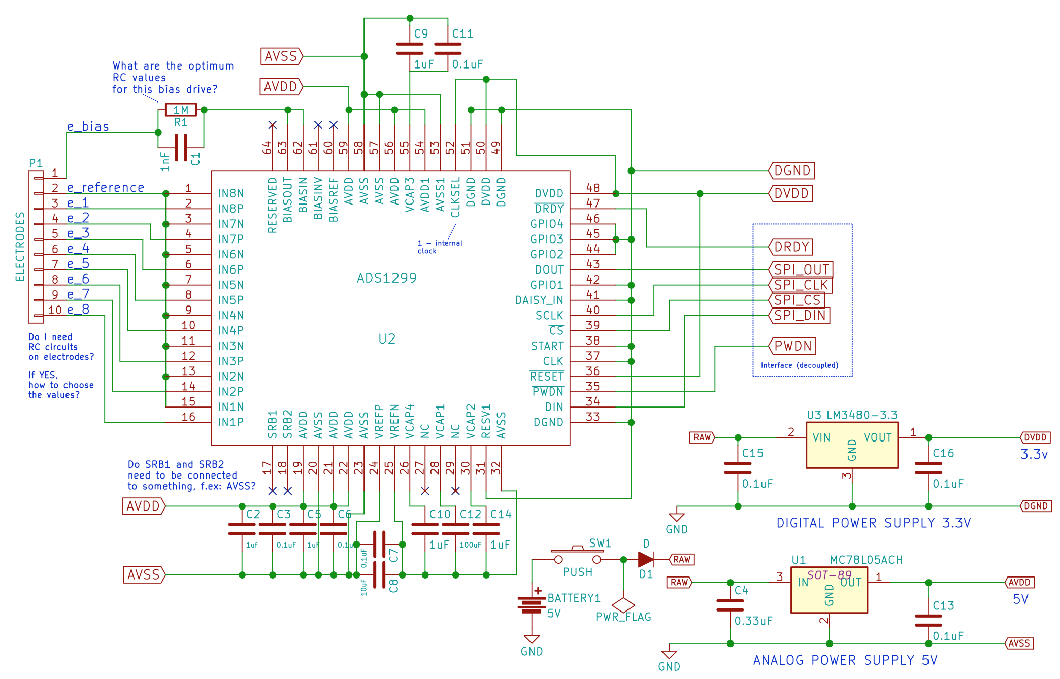
I am trying to design simplest schematics / PCB board for collecting EEG measurements using ADS1299.

This concept is based on ideas posted on this forum and inspired by :

Idea is:

  • The sensing electrodes are connected to positive inputs of all channels

  • The reference signal is fed to all negative inputs of the channels 1-8.

  • Use only BIAS_OUT pin of the ADS1299 without connection to the BIAS_INV. In this way you have open-loop amplifier in the feed-back loop of the first stage of the instrumentation amplifier. 
  • Must use battery power supply, or if you use USB or some wall adapter, use isolation DC/DC converter for patient safety and for better CMRR performance.

The author's claim is:
"With this configuration, you will get CMRR of 143dB and will have great EEG recordings without using Notch filter of 50/60Hz."

Could someone validate this and review my schematics (disclaimer: I am more of a software developer and just a electronics hobbyist noob)?

Other questions I have:

1. Do I need C1 capacitor (RC circuit) and why or is resistor enough?

2. Do I need RC circuit on sensing electrodes in this setup? I see those sometimes but not sure what is the purpose?

3. I am using a unipolar voltage power supply. Is there a difference in using this compared to bipolar one?

Would appreciate any help. It is my 1st question on this forum, and as I said - just a beginner -  so please be gentle ;-)

  • Hey Lukasz,

    Let me first give you some critiques on the schematic:

    • Leave the "CLK" pin open if unused. If you are using the internal clock, the CLK pin can be either an output or hi-z, so it's best to just float it.
    • From what I can tell, AVSS at pin 32 does not look like it is connected to other AVSS pins, but perhaps its connected by name and I have not seen it.
    • You can leave the SRB pins floating.

    About the author's strategy to maintain good CMRR, I'd like to understand more about the measurement setup. I am skeptical because if the device was configured to be in one of the settings where the input referred noise is roughly 1 uV, the noise level is at -133 dB from the reference voltage in the time domain. Now its possible that instead of measuring CMRR in the time domain that the author collected a lot of points and then analyzed them in the frequency domain where the noise floor can be pushed arbitrarily low by collecting more points and then looking for that signal power at 60 Hz, but the author doesn't specify how that value was measured.

    Another issue I have is leaving the bias amplifier in an open loop is that we wouldn't be able to specify its performance in saturation. All of the specifications for the bias amp are assuming closed loop operation. Instead it might be better to use a high closed loop gain rather than an open loop.

    Now I will answer your questions:

    1. That R and C will form a zero in the feedback loop formed by the electrode inputs to bias amplifier electrode at 1/(2piRC). You want to line up that zero with a pole that is formed by the electrode cable series resistance and shunt capacitance. That capactive loading could cause stability issued for the bias amplifier.
    2. It is good to put a simple RC filter for antialiasing. A cutoff >10 kHz is probably ok. Make sure, though, that the filter uses a differential capacitor between the channel inputs rather than common-mode capacitors. Component mismatch in common-mode RC filters could ruin your CMRR.
    3. There is no difference in performance. That decision is totally based on what is convenient for your power scheme.

    Regards,

    Brian Pisani