This thread has been locked.

If you have a related question, please click the "Ask a related question" button in the top right corner. The newly created question will be automatically linked to this question.

ADS8681EVM-PDK: interfacing with Microchip Micro controller on SPI bus

Part Number: ADS8681EVM-PDK
Other Parts Discussed in Thread: ADS8681

Sir,

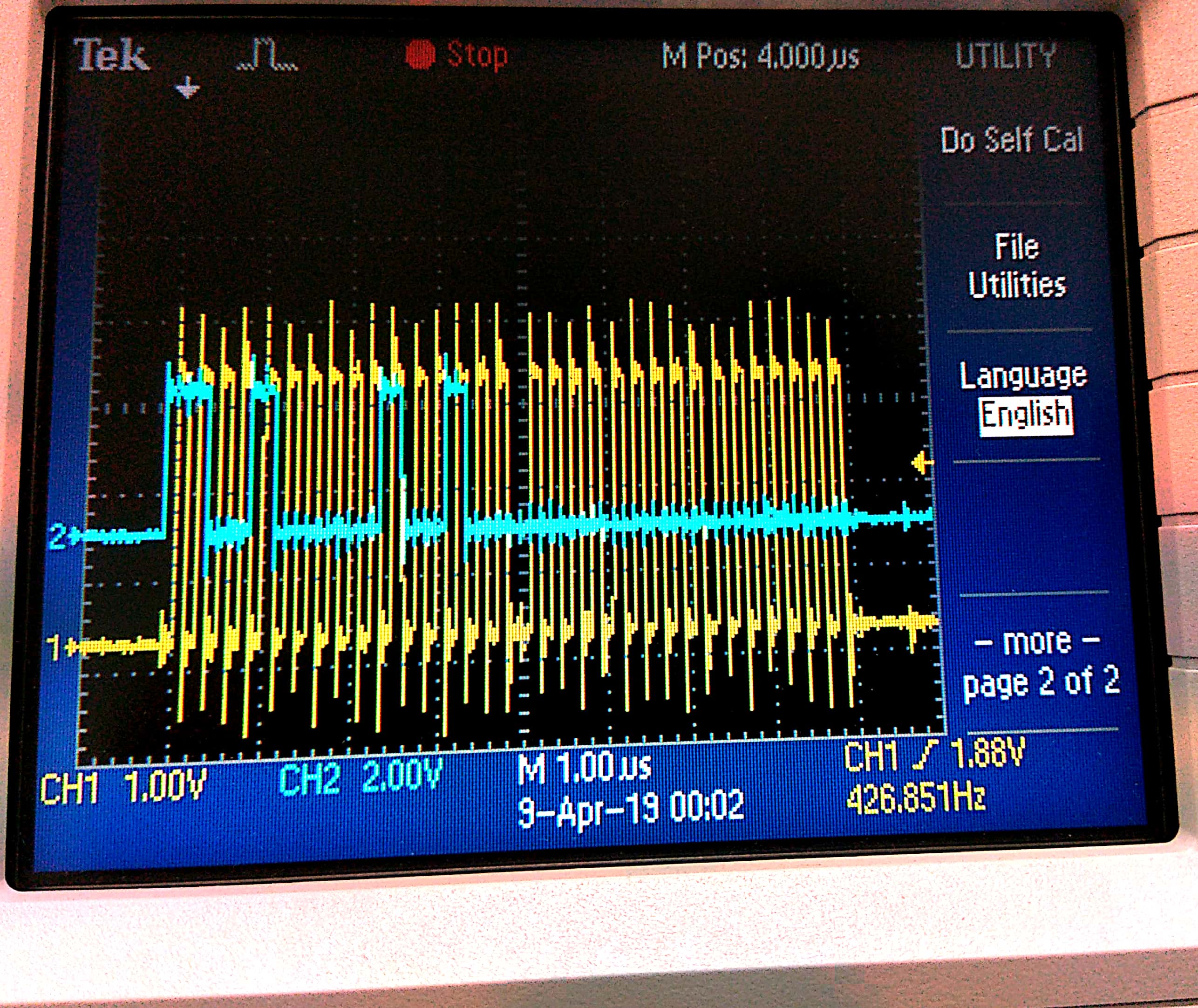
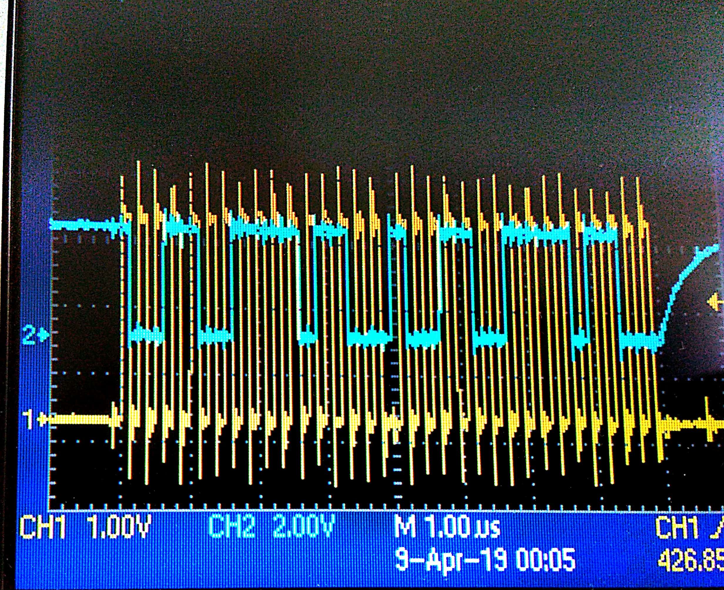
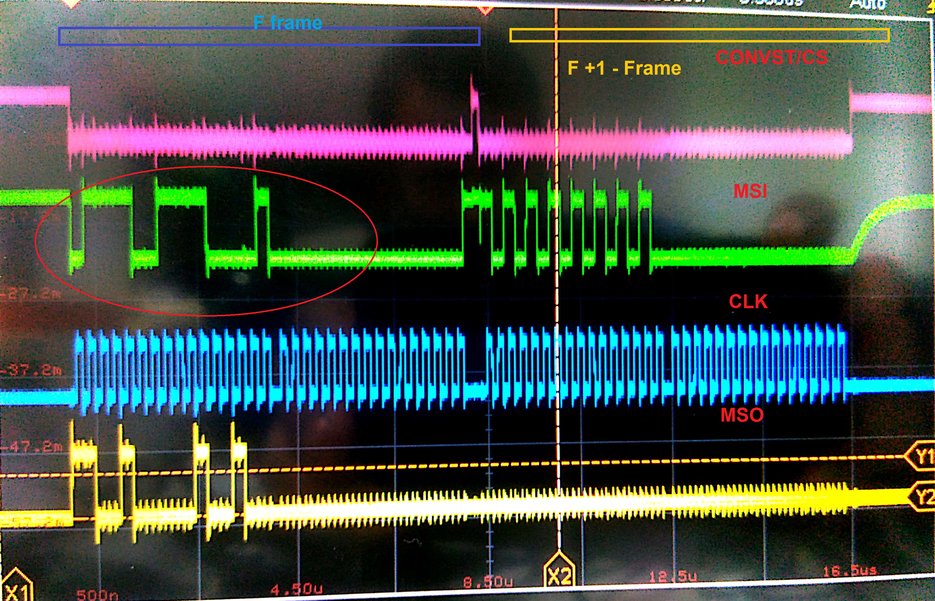
I am following the SPI protocol mentioned below for interfacing.

But, i am not getting proper data.

Example

1) Default Read of ALARM_H_TH_REG Register (address = 24h) is coming as 0x99eb. & This also random.

2) I am attaching the Code also here.

Pls suggest

Regards

Ramesh

  • I am adding flow

    1) Send ( WRITE COMMAND - 0xC800 | Register  Address : 0x24)

    2) Place 0x0000


    3) Read Data from SDI


  • Here , Read Value is not Proper. As per datasheet, it should get 0xFFFF.
    Pls Suggest
  • Sir,
    I have ADS8681EVM also. I am not finding the way to capture single Write Cycle / single Read cycle to correlate and correct my micro controller interface. Pls suggest
    -- Ramesh
  • Hi Ramesh,
    You command(0xC8240000) is right to read ALARM_H_TH_REG Register on ADS8681. Please notice the data on SDO from ADC should be checked in next frame. Did you pull up CONVST/CS pin back to high after sent out reading command? it will be good to have the timing plot with /SDI/SDO/SCLK and CONVST/CS together, also two timing frames will be better.
    To capture the writing timing on EVM board with PHI controller board, you can monitoring the SPI bus, then change the register content in "Register Map Config".
    Thanks.


    Regards,
    Dale

  • Dear Dali,

    1)

    Yes. Did you pull up CONVST/CS pin back to high after sent out reading command? - Gives me Right direction.

    " After Reading , CS made to go high" --- This helped me.

    2) Datasheet is not clear that which  register i should read to get the Analog converted Value?

    -- Ramesh


  • Hi Ramesh,
    To read internal register, a READ_HWORD or READ command with proper address and format can be sent to ADC in frame F, the output data for frame (F+1) will contain 16-bit register data followed by 0's, so we have to check the data in next frame (F+1). Since the command provided in frame F will get executed at the rising of CONVST/CS signal, this is why I asked the question.
    To get the conversion data from this ADC, there is no register to read. For any command except READ_HWORD or READ, the ADC will output 16-bit conversion result in next frame (F+1). Please see the description on page 44 of ADS8681 datasheet. The ADC only needs clocks on SPI to output the conversion result after conversion is finished(wait for tconvst_max or monitor RVS signal), so a NOP can be used as well in frame (F+1). Please see the timing in Figure 5 ~6 of datasheet.

    Thanks&regards,
    Dale

  • I want to update further based on your suggestion,

    I do not have logic scope, capturing via CRO.

    My microcontroller supports 16 bit SPI transaction, 32 bit not available.

    CODE

    1) Initialization

    qspi_initialize(QSPI,&mode_config); // load the configurations in register

    printf ("\r SPI Master Mode \n");
    ads8681_reg_write(0x24,0xAAAA); // just bring data on CRO

    2) Loop

    while(1)
    {

    data_16 = 0;
    ads8681_reg_read(0x24,&data_16);

    printf("\r SPI READ Mode ADD : 0x%x : 0x%x\n",0x24,data_16);

    delay_us(600);


    }


    3) 

    Read function 

    status_code_t ads8681_reg_read(uint16_t add,uint16_t *data_pt)
    {

    status_code_t status = STATUS_ERR_BUSY;

    /* Write command -1 st 32 bit */
    qspi_chip_select(0);
    qspi_write_spi(CMD_READ_HWORD | add );
    qspi_write_spi(0x0000);
    qspi_chip_select(1);

    /* Dummy write 2nd command */
    qspi_chip_select(0);
    qspi_write_spi(CMD_NOP );
    qspi_write_spi(0x0000);
    (*data_pt) = qspi_read_ads();
    qspi_chip_select(1);


    return status;

    }


    Query

    1) I have marked red in circle , Is it unwanted , / OR it is coming due to while loop in the code?

    2) I am getting the data on Second frame by giving NO OP command. Is it Ok?

    3) For Reading the Conversion Data , 

    " For all other combinations, the output data word for frame (F+1) contains the latest 16-bit conversion result.
    Program the DATAOUT_CTL_REG register to append various data flags to the conversion result. The data
    flags are appended as per following sequence:"

    I can make any command other than the list mentioned in the data sheet Table -5 , Then i will get the Result on F +1 frame which i marked in  my pics

    Is it OK?

    Pls put your answer number wise to make more understanding


    Regards

    Ramesh

  • 4) For command for conversion is , I took 0x3000. ( other combination of command), them i try to read dummy.
    Always getting Fixed value (F+1) , even though input amplitude is changed.
    Pls suggest
  • Hi Ramesh,
    I will check the detail and get back to you soon. Thanks.

    Best regards
    Dale
  • Dear Dale,

    1) One success , i have got.

    2) I send ( CMD_WRITE_HWORD | DATAOUT_CTL_REG ) in F - frame , Then in the next frame (F+1) , i have got the data which vaying when i give external input to ADC pin.

    3) Is this command format  right to read the conversion result?

    ( here note  CMD_WRITE_HWORD  = 0xD000 , DATAOUT_CTL_REG_ADD  = 0x10)

    Regards

    Ramesh

  • Hi Ramesh,

    Firstly, the signal name in your timing plot confused me. I think your "MSI" signal should be MISO which is the output (SDO) from ADC to your microcontroller. Also, your "MSO" should be MOSI which is the signal for sending the command from microcontroller to ADC (SDI). Please correct me if my understanding is wrong.

    1) I think it is the output data and related to your previous command.

    2) You have two questions in your two different posts:

    To answer your question " I am getting the data on Second frame by giving NO OP command. Is it Ok?", yes.

    The latest timing you showed is correct, you can see the register value of ALARM_H_TH_REG Register was shifted out to SDO line(MSI) by the ADC with first 16 clocks during frame (F+1), ithe value is 0xAAAA which is correct, the reason why you got the ALARM_H_TH_REG Register content not default 0xFFFF is you have changed the content of this register by writing "reg_write(0x24,0xAAAA)" command during your code Initialization. Hence, both your command and timing are correct, and the ADC is working well.

    For your second query about "I send ( CMD_WRITE_HWORD | DATAOUT_CTL_REG ) in F - frame , Then in the next frame (F+1) , i have got the date which vaying when i give external input to ADC pin.", this is correct that the conversion data will be shown in frame(F+1) for all other combination commands. For the reason about "your data is varying", I'm not sure if your signal source is stable or how much code variation you got. Actually, you can disconnect ADC's analog input and check the conversion code, I can help you check if you can send the code to me.

    3) Actually, the conversion data can be read without commands during same frame F. Please see the Figure 3 or 4 in ADS8681 datasheet, When CONVST/CS pin is pulled down to low, the ADC starts the conversion, the RVS signal from low to high indicates that the ADC conversion has been finished, the ADC enters acquisition period and the conversion data is ready to read with clocks on SCLK.

    Let me know if you have any further question, thanks.

    Best regards,

    Dale