This thread has been locked.

If you have a related question, please click the "Ask a related question" button in the top right corner. The newly created question will be automatically linked to this question.

ADS54J66: ADS54J66: the jesd204B sync process

Part Number: ADS54J66


Hi Jim

 the ADS54J66 in DDC mode 8  with LMFS = 4421 .

 The SYSREF is 7.8125MHz(128ns) and the ADC devclk is 500MHz,  FPGA devclk is 250MHz.

the write squence is shown below:

{ 0x0000, 0x81 },

{ 0x4004, 0x68 },
{ 0x4003, 0x00 },
{ 0x60F7, 0x01 }, //Self-clearing reset for the digital block. AB channels
{ 0x60F7, 0x00 }, //
{ 0x70F7, 0x01 }, //Self-clearing reset for the digital block. CD channels
{ 0x70F7, 0x00 }, //

//Analog bank master page (80h)
{ 0x0011, 0x80 }, //choose master page
{ 0x0053, 0x80 }, //clk divided-by-2
{ 0x0039, 0xC0 }, //ALWAYS WRITE 1
{ 0x0059, 0x20 }, //ALWAYS WRITE 1

//JESD bank 6800h IL pulse
{ 0x6000, 0x01 },
{ 0x6000, 0x00 }, //pulse.Interleaving engine reset, 6800h takes effect. AB channels
{ 0x7000, 0x01 },
{ 0x7000, 0x00 }, //pulse.Interleaving engine reset, 6800h takes effect. CD channels

//JESD bank decimation filter page(6141h)
{ 0x4004, 0x61 }, //choose decimation filter page
{ 0x4003, 0x41 },
{ 0x6000, 0x08 }, //Mode 8. No decimation, no mixing, straight 500-MSPS data output. AB channels
{ 0x7000, 0x08 }, //Mode 8. No decimation, no mixing, straight 500-MSPS data output. CD channels
{ 0x6001, 0x04 }, //always write. AB channels
{ 0x7001, 0x04 }, //always write. CD channels

//JESD bank analog page(6A00h)
{ 0x4003, 0x00 },
{ 0x4004, 0x6A }, //choose analog page(6A00h)
{ 0x6016, 0x02 }, //JESD PLL MODE: 40x mode. AB channels. the register description is wrong
{ 0x7016, 0x02 }, //JESD PLL MODE: 40x mode. CD channels. the register description is wrong


//JESD bank digital page(6900h)
{ 0x4003, 0x00 },
{ 0x4004, 0x69 }, //choose digital page(6900h)
{ 0x6000, 0xC0 }, //Enable JESD MODE control. AB channels
{ 0x6001, 0x01 }, //JESD MODE 20x mode for LMFS = 4421. AB channels
{ 0x7000, 0xC0 }, //Enable JESD MODE control. CD channels
{ 0x7001, 0x01 }, //JESD MODE 20x mode for LMFS = 4421. AB channels
{ 0x6006, 0x0F },
{ 0x7006, 0x0F },

//Analog bank ADC page(0Fh)
{ 0x4005, 0x01 },
{ 0x7001, 0x21 } //JESD MODE 20x mode for LMFS = 4421. AB channels

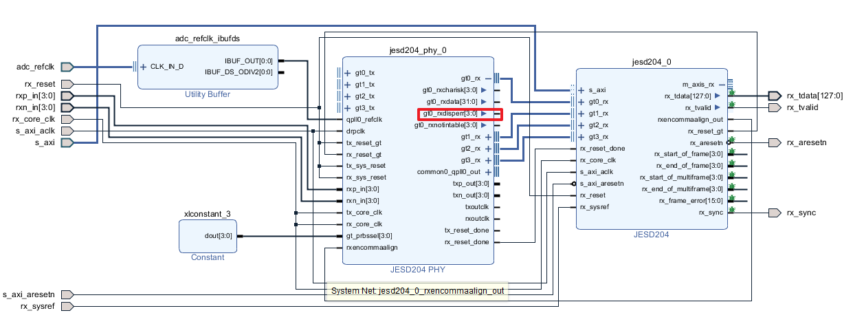
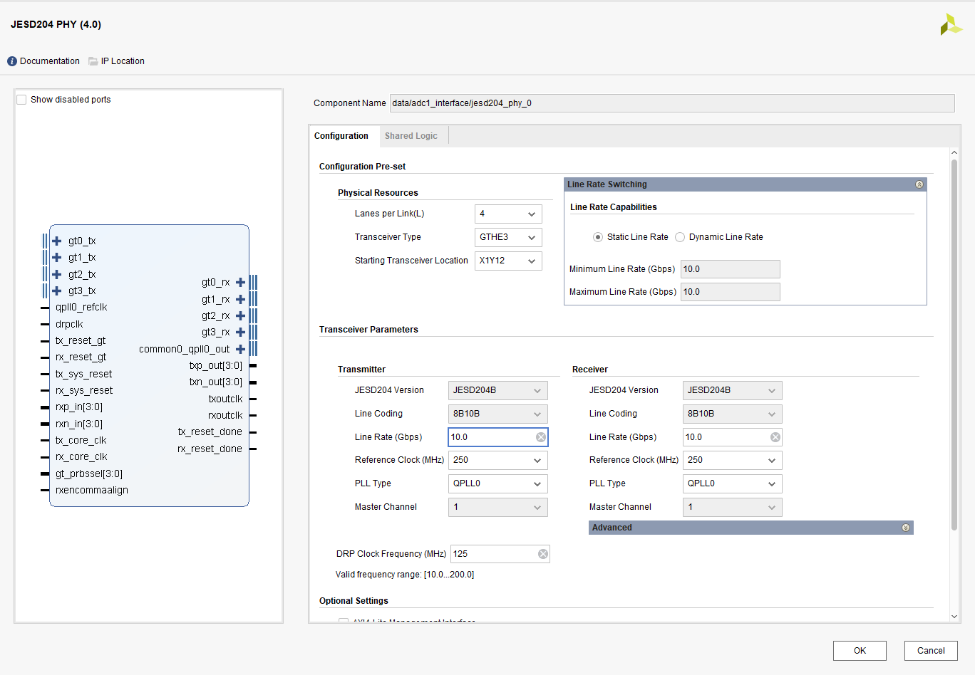
In FPGA , I use the IPcore  jesd204_phy with 10Gsps Line Rate  and the IPcore   JESD204 with F=2, K=16.

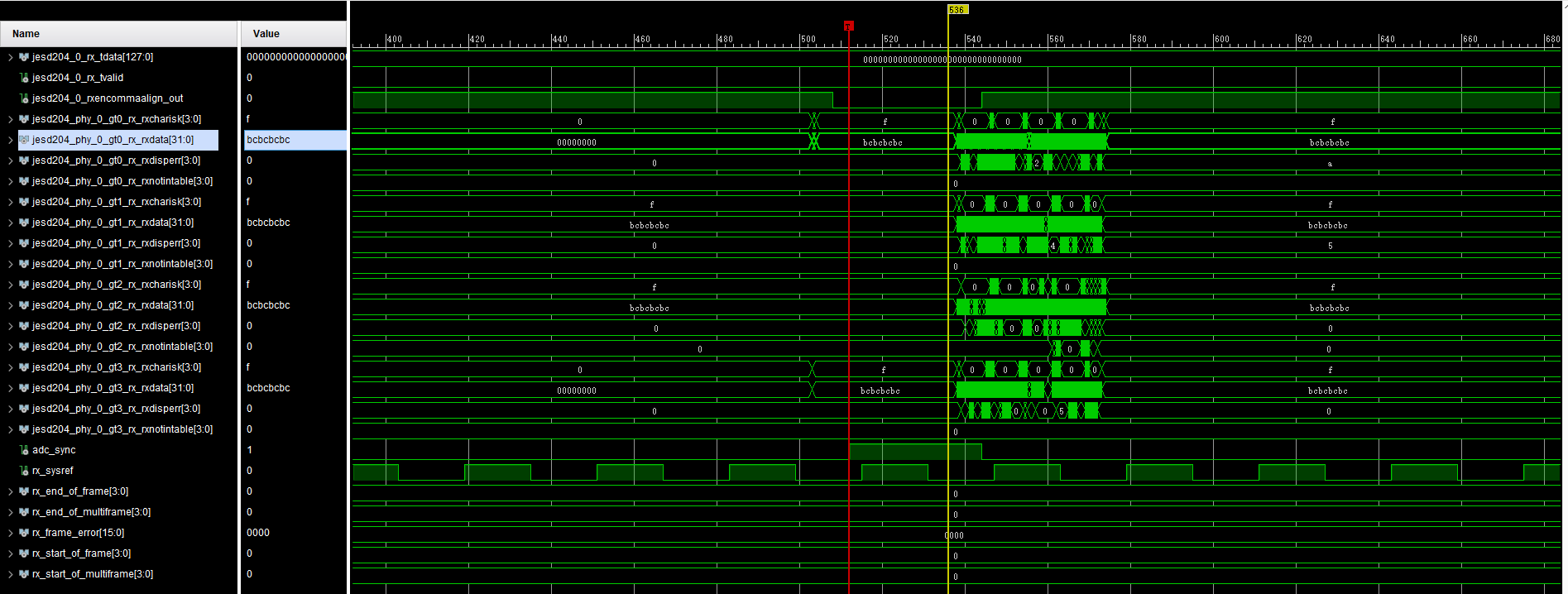
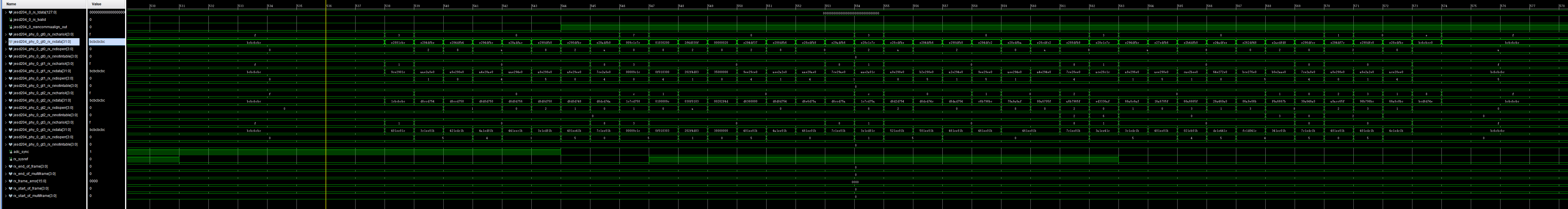
After receiving  K28.5 symbols  in succession,  the IPcore JESD assertes the rx_sync signals. However, it will de-assert the  rx_sync signals in 22 devclk cycles. the debug wave is shown in below.

After the  ILA squence, the gtx_rx_rxdata[31:0] is still "bcbcbcbc", but gtx_rx_disperr[3:0] is not "0", which won't assert the rx_sync signal any more. 

Can you help me about that?

Best regards.

  • The pictures can not appear above,  so I add it again.

    user6050741 said:

  • What is gtx_rx_disperr[3:0]?

  • Hi Jim

    I use the jesd204_phy and jesd204 to receive the adc data.

    The jesd204_phy provides the signal gtx_rxdisperr[3:0] to the jesd_204 to  indicate disparity error in each lane.

    their datasheet is pg195 and pg066.

    https://www.xilinx.com/support/documentation/ip_documentation/jesd204_phy/v4_0/pg198-jesd204-phy.pdf

    https://www.xilinx.com/support/documentation/ip_documentation/jesd204/v7_2/pg066-jesd204.pdf

    Two IPcores are used as the following: 

    How do you receive the jesd204B data if you don't use these two IPcore?

  • Go to the TSW14J10EVM product folder on the TI website for example source code we used to interface the ADS54J66EVM with Xilinx platforms.

    Regards,

    Jim

  • Hi,

    this is probably a long shot, but we were seeing the same disparity errors with your configuration. Replacing

    //JESD bank digital page(6900h)
    { 0x4003, 0x00 },
    { 0x4004, 0x69 }, //choose digital page(6900h)
    { 0x6000, 0xC0 }, //Enable JESD MODE control. AB channels
    { 0x6001, 0x01 }, //JESD MODE 20x mode for LMFS = 4421. AB channels
    { 0x7000, 0xC0 }, //Enable JESD MODE control. CD channels
    { 0x7001, 0x01 }, //JESD MODE 20x mode for LMFS = 4421. AB channels
    { 0x6006, 0x0F },
    { 0x7006, 0x0F },

    with

    //JESD bank digital page(6900h)
    { 0x4003, 0x00 },
    { 0x4004, 0x69 }, //choose digital page(6900h)
    { 0x6000, 0x40 }, //Enable JESD MODE control. AB channels
    { 0x6001, 0x01 }, //JESD MODE 20x mode for LMFS = 4421. AB channels
    { 0x7000, 0x40 }, //Enable JESD MODE control. CD channels
    { 0x7001, 0x01 }, //JESD MODE 20x mode for LMFS = 4421. AB channels
    { 0x6000, 0x80 }, //custom K
    { 0x7000, 0x80 }, //custom K
    { 0x6006, 0x0F },
    { 0x7006, 0x0F },

    i.e. setting mode and K in two sperarate writes, solved the issue for us.

    Best regards,
    David

  • David

         Your configuration does clear the disparity errors.   

         Thank you for your help. 

         Best regards.

  • Hi,

    I'm facing issues with rx_sync. Here is the initialization sequence I am following - 

    1) Program LMK and wait for PLL2 Lock.

    2) Program FPGA

    3) Send 1 to rx_reset pin of the JESD RX module.

    4) Send 0 to rx_reset pin of JESD RX module.

    5) Write 0x2 to JESD RX AXI register 0x04 (fixed reset) to hold the JESD core in reset.

    6) Program ADC registers.

    7) Clear JESD core reset. After clearing reset, the GT lanes start seeing 0xBCBC characters.

    8) Trigger Sysref

    Could you please share the initialization sequence you are following. Thank you

  • Hi

    A continuous SYSREF is used in my work.

    Here is the initialization sequence I am following -

    1) Program FPGA

    2) Program LMK and wait for PLL2 Lock. Both DEVCLK and SYSREF are provided.

    3) Program ADC registers.(The configuration of some registers requires the existence of sysref)

    4) Send 1 to rx_reset pin of the JESD RX module.

    5) Send 0 to rx_reset pin of JESD RX module.

    Hope this will help you!

  • User,

    I agree with most of the steps above. The only difference I would make is to program the LMK first programming the FPGA. Sometimes the FPGA logic needs clocks before registers are programmed.

    Regards,

    Jim