This thread has been locked.

If you have a related question, please click the "Ask a related question" button in the top right corner. The newly created question will be automatically linked to this question.

CCS/ADS1231REF: Problem w/ data rate of ADS1231REF and receiving accurate codes in receive buffer of MSP430F5529LP

Part Number: ADS1231REF
Other Parts Discussed in Thread: ADS1231, MSP430F5529, MSP430F449, ADS1232REF

Tool/software: Code Composer Studio

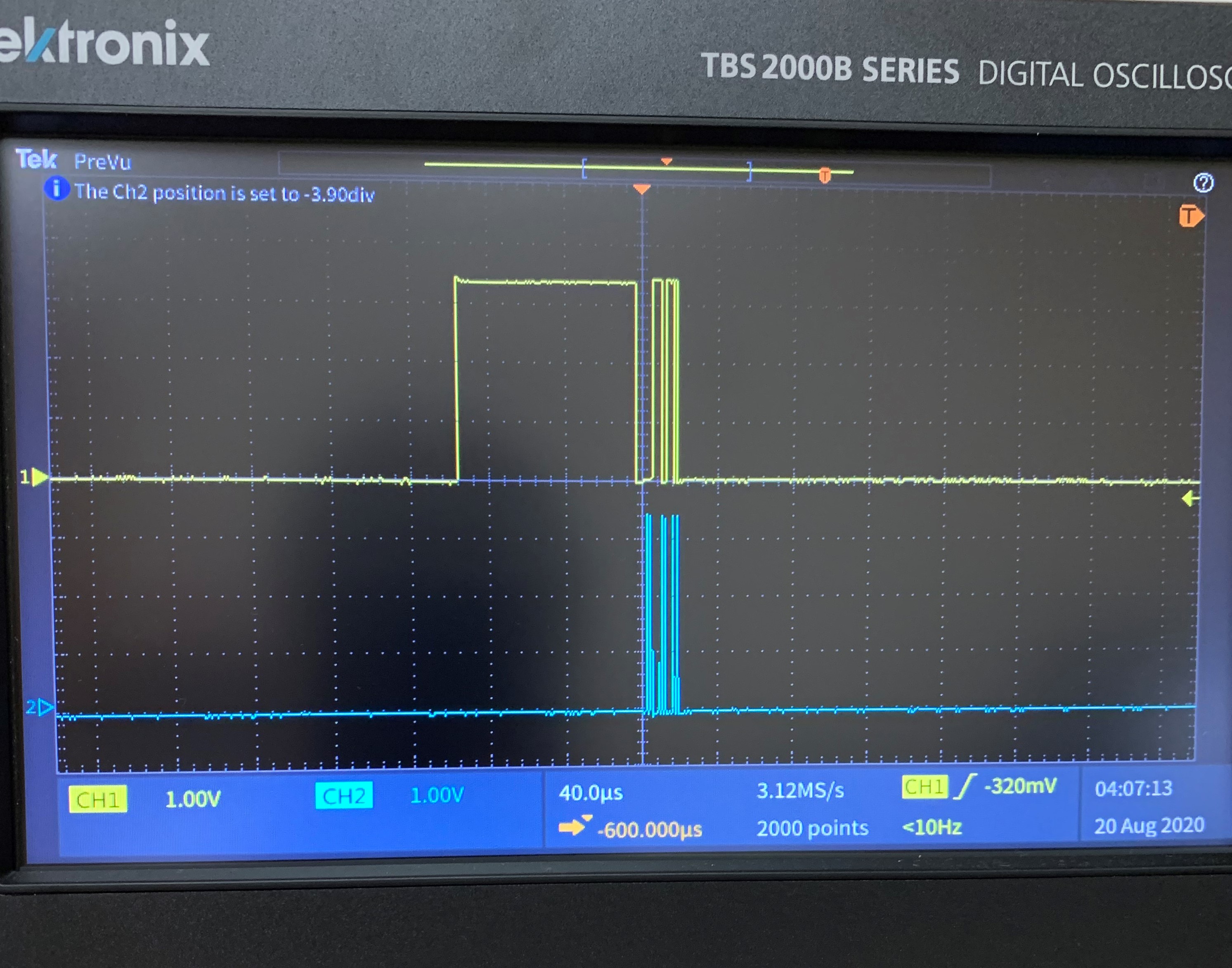
According to the timing diagram on p.13 of ADS1231's datasheet, the total time for all 24 bits of data to output (t_conv) should be 12.5 ms when SPEED is high, which I have configured on my ADS1231REF board. However, my oscilloscope shows the signal functioning otherwise. Why is one bit of data roughly 12.5 ms long when all 24 bits should be outputted in that duration? How can I speed up my board's data output?

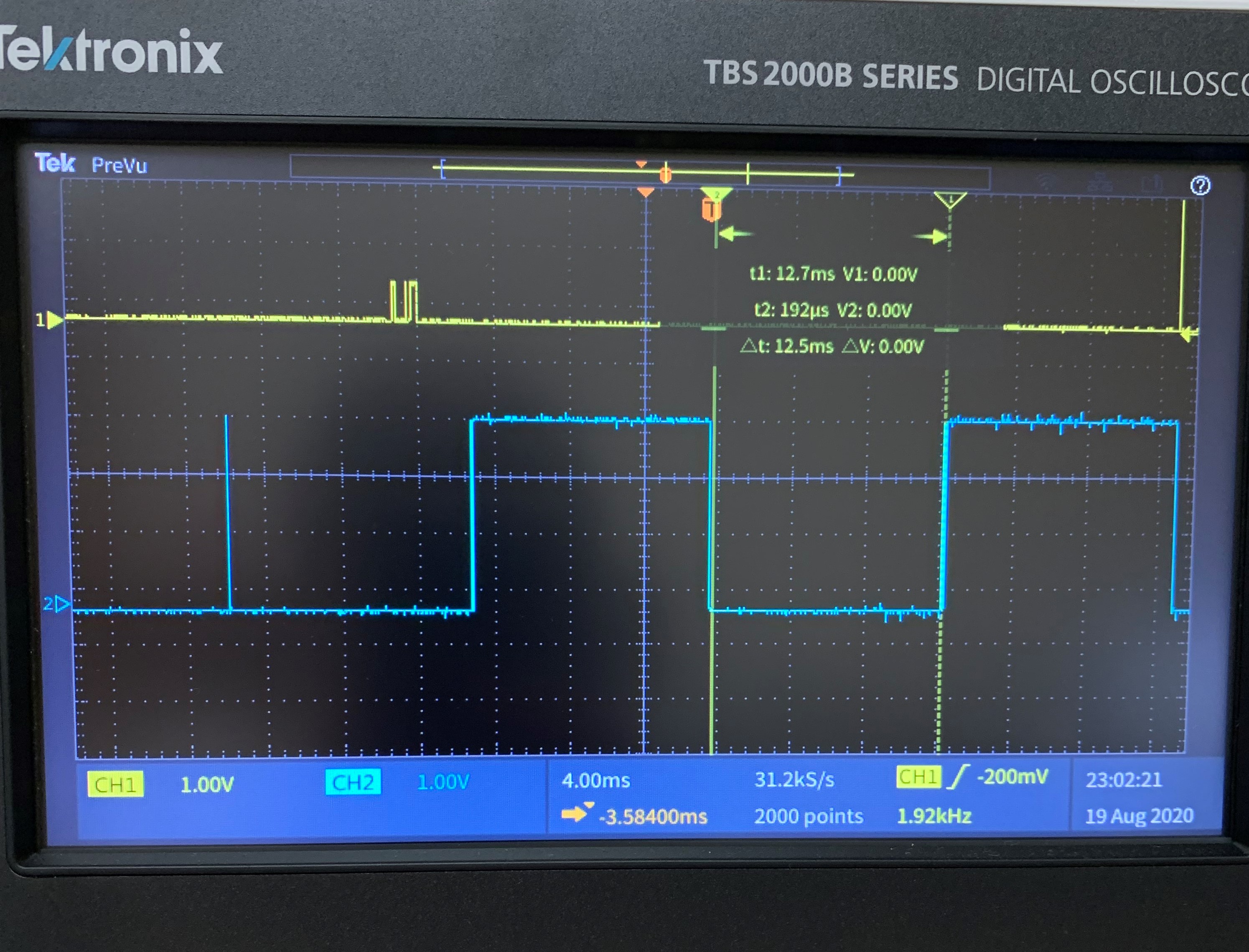
Below is a picture of the oscilloscope. As you can see, the duration of one low bit is roughly 12.5 ms. Here, SCLK is running at 32,768 Hz, and all 8 pulses are generated within only 1 bit of data output. So, the data my program obtains at this clock setting is mostly 0xffffff.

When I set SCLK to roughly 80 Hz (79.92 Hz) to synchronize with the data rate of the ADS1231REF, this is the data I receive. It is very inconsistent and does not translate to the actual expected data. 

DEBUG POINT: The code is 10d8dec
DEBUG POINT: The code is bd3dba
DEBUG POINT: The code is e767d5
DEBUG POINT: The code is 9b1b0f
DEBUG POINT: The code is 8f0fdc
DEBUG POINT: The code is 9f1fc2
DEBUG POINT: The code is 84048a
DEBUG POINT: The code is 1028269
DEBUG POINT: The code is 9a1a9d
DEBUG POINT: The code is df5f8a
DEBUG POINT: The code is d050db
DEBUG POINT: The code is 10f8fda
DEBUG POINT: The code is 15ddd86
DEBUG POINT: The code is ff7f47
DEBUG POINT: The code is 127a7ea
DEBUG POINT: The code is 10b8bbb

Is there a problem with my program? Below is the function in my code that gets the 24 bit code from the ADS1231.

int32_t get_Code(void)
{
    int32_t code, data1, signExtension;
    int16_t data2;
    int8_t data3, sign;

                                      //new data is ready to be outputted when DRDY (P7.0) goes low. then, on the first rising edge of SCLK, data is shifted out bit by bit
    while (P7IN & BIT0); // exits loop when P7.0 (DRDY) goes low / new data is ready

    while (!(UCB0IFG & UCTXIFG));
    UCB0TXBUF = 0x21;


    data1 = UCB0RXBUF;
    sign = data1 >> 7;
    if (sign) signExtension = 0xff;
    else signExtension = 0x00;
    signExtension <<= 24;
    data1 = data1 << 16;


    while (!(UCB0IFG & UCTXIFG));
    UCB0TXBUF = 0x22;
    while (!(UCRXIFG));
    data2 = UCB0RXBUF;
    data2 = data2 << 8;


    while (!(UCB0IFG & UCTXIFG));
    UCB0TXBUF = 0x23;
    while (!(UCRXIFG));
    data3 = UCB0RXBUF;


    while (!(UCB0IFG & UCTXIFG));
    UCB0TXBUF = 0x24; // 25th SCLK cycle to set DRDY high

    code = data1 + data2 + data3 + 0x800000;                //to make ADC codes unipolar
    code &= 0x00ffffff;
    printf("DEBUG POINT: The code is %04lx\n", code);

    return code;
}

  • Hi Yamen,

    I read through your other post found here:

    https://e2e.ti.com/support/microcontrollers/msp430/f/166/t/928115

    To summarize, you are connecting an MSP430F5529 LaunchPad (LP) to the ADS1231REF board.  You are connecting the LP connections directly to the ADS1231REF test points.  This places the onboard MSP430 in direct contention with the LP.  Your solution sounds reasonable by holding the onboard MCU in reset, however, the reset switch also controls the enable pin on the 3.3V LDO used to power the digital portion of the ADS1231REF.  Also, you must make sure that the PDWN pin does not float.

    So you must add the connection to pull the PDWN pin high, and disconnect the SCLK, DOUT, SPEED and PDWN pins from the onboard MCU.  One way is to carefully cut the traces at the TPs to disconnect the communication from the MCU.  Also, do not press and hold the RESET switch.  Removing the digital supply and then driving the inputs will cause excessive current to flow through the digital input pins which could damage the ADS1231.  Before breaking any connections to the onboard MCU I would recommend that you observe the communication from the onboard MCU to see what it should like like in the capture operation.

    Another issue is you need to connect the ground of the ADS1231REF to the ground of the LP.

    Lastly, you need to capture the conversion result within the time between the completion of each conversion.  To do so you need a faster SCLK.  The SCLK can go as fast as 5MHz, but I would suggest using something in the range of 1 to 2MHz.  The goal here is to completely read the conversion result before the next conversion result completes.  For this ADC, the internal oscillator drives the conversion clock.  The conversion is not related to the SCLK like many SAR ADCs.

    Best regards,

    Bob B

  • I'm a little confused. By the launchpad, do you mean the MSP430F5529 MCU that is attached to the 40 pin header? And by the onboard MCU, do you mean the ez-FET emulator?

    Being that the holes labeled DOUT, SCLK, etc. on the ADS1231REF are testpoints, are you not able to input signals? For example, how will the SCLK signal generated by the LP be sent to the ADS1231REF if the traces are cut and communication is disconnected?

    I soldered a wire to the PWDN testpoint, connected it to P2.2 of my LP, and set the output high. I also connected the ground of the ADS1231REF to the ground of the LP.

  • Hi Yamen,

    I'm not talking about the emulator.  The ADS1231REF has an MSP430F449 on the board to control the ADS1231 on the ADS1231REF board.  The test points are monitoring points.  When you connect the MSP430F5529 LaunchPad to the ADS1231REF, both MCUs are competing against each other. 

    So you need to cut or remove the communication from the onboard MSP430F449 from the ADS1231.  You cannot have both the MSP430 devices connected to the ADS1231 at the same time.  I suggested that before you break the connections you monitor the output of the MSP430F449 to see what the communication should look like.

    Best regards,

    Bob B

  • Oh okay, I understand the difference now.

    How can I monitor the output of the MSP430F449? Shouldn't I be able to see the SCLK signal generated by the MSP430F449 when I disconnect the testpoints from my LP? Instead, I get a flat line.

    What can I cut the traces with? I'm assuming I should cut where they lead to the MSP430F449 from the testpoints.

  • Hi Yamen,

    Yes, you should be able to able to see the SCLK at the test point assuming that nothing was damaged in the process when you applied signals and held the RESET switch low.  Do you see the LCD display updating at all?  If it is, then you should be able to see the SCLK.

    Best regards,

    Bob B

  • I believe the SCLK and DOUT signals are working as intended using the onboard MCU. I've attached an image of my oscilloscope below. The blue signal is SCLK and the yellow is DRDY/DOUT. Before each bit is shifted out, DRDY/DOUT goes high for a signfiicant amount of time. I assume this is because new data is not yet ready to be outputted. Then, DRDY transitions low when the new data is ready, and begins to shift serially at each rising edge of SCLK.

    In my previous setup, did the clock signal that was generated by the LP never reach the ADS1231REF when the SCLK test point was directly connected to the pin header? I'm trying to figure out why the ADS1231REF is now able to synchronize with the rising edges of SCLK, while before each bit of data outputted from DOUT was always 12.5 ms per bit regardless of SCLK. This is why I previously set the LP's clock output to be 80 Hz.

  • Hi Yamen,

    The timing you show in the scope plot for the yellow trace is showing the update period where the conversion result is being written to the output buffer of the ADS1231. The datasheet timing diagram in Figure 19 shows the typical update period (tUPDATE) as 90us.  Your scope is set to 40us per division, so we see the update period matches pretty well.

    The data should be read from the device as soon as it becomes available.  The firmware uses a GPIO that has a high-to-low edge triggered interrupt that gets triggered to read the conversion result.

    When you connected the LaunchPad to the ADS1231, the micro outputs were competing with one another.  You cannot connect two outputs together at the same time.  Also, if you press the RESET switch the LDO for the digital supply is also disabled.  With the digital power off from supplying DVDD to the ADS1231, the ADS1231 then randomly gets powered from digital I/O that back drives current through the ESD structures on the input pins.  This violates the absolute maximum ratings for the ADS1231.  You will get odd behavior for this type of input conditions. 

    Best regards,

    Bob B

  • So to prevent the micro outputs from competing with one another, I must cut the traces leading to the onboard MCU from each of the the DOUT, PWDN, SCLK, and SPEED test points. Then, I will be able to control the ADS1231 solely from my LP. How should I cut the traces?

    In my code, I send a fourth dummy value to the transfer buffer to generate a 25th clock cycle and set DRDY high, and then I have a few lines of code to calculate the 24 bit code and clear the interrupt flag. By the time I exit the ISR and am ready to re-enter it, will the DRDY signal already have gone low because new data is ready so the interrupt won't trigger on a HIGH to LOW transition?

  • Hi Yamen,

    To cut the traces, you need something sharp that can cut through the copper.  I have used a hobbyist knife like might be used in artwork or building models.  I have also used a sharp tool, like a dental tool or a small awl to scrape the copper trace away from the pad. You will also probably need a magnifying glass.  Be very careful not to hurt yourself in the process.

    If you use an interrupt routine you do not need to send the extra byte of SCLKs to force DOUT/DRDY high.  You would only need to do this if you are polling the pin.  When the conversion completes, there is always an update period.  If the DOUT/DRDY is already high from the last bit of data transmitted, you will see the signal transition low.  If the DOUT/DRDY is low, then you would see the pin pulse from low-to-high-to low signaling the new result is ready.  So there should always show a high-to-low transition after every conversion.

    As far as your timing, I cannot say how long it takes for you to run your routine, but you should be able to easily capture the results for each conversion.  At 80sps you have 12.5ms to work with to capture the data and re-enter normal code flow.  As I recall, the LP is running 3 times faster than the onboard micro where there is plenty of time to capture and display the conversion data for each conversion result.

    Best regards,

    Bob B

  • I was able to cut the traces leading to the onboard MCU from the DOUT and SCLK test points. The signals on the oscilloscope make much more sense now, but I've run into another problem. In order to calibrate the scale, I measure the code and weight with no load on the scale and with a predetermined calibration mass that is inputted into the program. Then, I am able to calculate the weight in grams on an infinite loop based on the values obtained during calibration. However, these are the results I'm receiving.

    Your weight is 38.58728.
    Your weight is 54.12695.
    Your weight is 54.47614.
    Your weight is 40.20233.
    Your weight is 57.00787.
    Your weight is 421.2299.
    Your weight is 38.58728.
    Your weight is 38.41266.
    Your weight is 1801.292.
    Your weight is 45.70233.
    Your weight is 37.9325.
    Your weight is 37.9325.
    Your weight is 37.9325.
    Your weight is 37.9325.
    Your weight is 37.9325.
    Your weight is 37.9325.
    Your weight is 37.9325.

    As you can see, after about ten calculations, my program is stuck. Here are images of my oscilloscope during the first ~10 measurements (when it's working) and after it gets stuck.

  • Hi Yamen,

    Something is not correct in the way DOUT/DRDY line output looks.  I see many long series with no new conversion data.  I would suggest checking to make sure that the system is working as expected by not sending SCLKs to retrieve data.  Based on the SPEED setting, you should either see DOUT\DRDY toggling every 100ms or every 12.5ms (except for the very first conversion after power-up where the first output requires 4 conversion cycles of the digital filter to settle).  There are many periods where there are long stretches as much as 400ms.  This leads me to believe you have some connection issues with PDWN or SPEED or both.  Or it is possible that you do not have the ground of the ADS1231REF connected to the ground of the LaunchPad.

    Best regards,

    Bob B

  • Hi Yamen,

    Also your code has issues.  I thought you said it was interrupt driven?  It is actually polling.  Also when you collect the data, you need to make sure that you have waited for the transmission cycle to complete before attempting to read the data.  I think you are missing this for data1.  And it is not clear what you are trying to do with sign extension at the top.  However I see that you are trying to convert the result to a unipolar value.

    Best regards,

    Bob B 


  • Hi Bob,

    Now my ADS1231REF board won't output any data, even if the program is running and SCLKs are generated. Previously, I had just cut the traces for the DOUT and SCLK test points, but after your most recent reply, I went ahead and cut the trace next to the PWDN test point as well. However, my oscilloscope isn't measuring any signal from DOUT, just that it is continuously set high. Attached is a picture of the back of my board. The circle on the right shows where I cut the traces for SCLK/DOUT and the circle on left shows PWDN. I used a multimeter to check whether the connections were in fact disrupted.

    Also, the code I originally posted is not the updated code I've been working with, sorry about that. Below is interrupt service routine I use to collect the data.

    #if defined( __TI_COMPILER_VERSION__ ) || defined( __IAR_SYSTEMS_ICC__ )
    #pragma vector = PORT1_VECTOR
    __interrupt void Port_1(void)
    #elif defined(__GNUC__)
    void __attribute__ ( (interrupt(PORT1_VECTOR) ) ) Port_1 (void)
    #else
    #error Compiler not supported!
    #endif
    {
        int32_t data1;
        int16_t data2;
        int8_t data3;

        switch ( __even_in_range( P1IV, P1IV_P1IFG7 ))
        {
            case P1IV_P1IFG1:
            is_ready = true;
            P1IFG &= ~BIT1; // clear interrupt flag
            break;

            case P1IV_P1IFG3:
            while (!(UCB0IFG & UCTXIFG));
            UCB0TXBUF = 0x21;
            while (!(UCRXIFG));
            data1 = UCB0RXBUF;
            data1 = data1 << 16;

            while (!(UCB0IFG & UCTXIFG));
            UCB0TXBUF = 0x22;
            while (!(UCRXIFG));
            data2 = UCB0RXBUF;
            data2 = data2 << 8;

            while (!(UCB0IFG & UCTXIFG));
            UCB0TXBUF = 0x23;
            while (!(UCRXIFG));
            data3 = UCB0RXBUF;

            code = data1 + data2 + data3 + 0x800000;
            code &= 0x00ffffff;

            P1IFG &= ~BIT3; // clear interrupt flag
            break;

        }

    }

  • Hi Yamen,

    Where you cut the traces looks to be correct.  I do see that the SCLK solder joint seems to be poor and perhaps is not a good connection.

    The SPEED pin cannot be floating, so check the voltage to make sure that it is at the appropriate level.  If you monitor DOUT/DRDY you should see this toggling at the data rate (SPEED) selected.  If DOUT is always high, then I would make sure that the PWDN pin is set to logic high.  If PWDN is low, the ADS1231 will be in the power down state.  Also make sure that SCLK is dwelling low.  If SCLK is dwelling high, the the ADS1231 will go to sleep.

    How are you now powering the ADS1231REF board?  Both the analog and digital supplies must be at nominal operating voltage or the ADS1231 will be held in a reset state.

    Best regards,

    Bob B

  • The PWDN pin was somehow set low, so I modified the code and now the board is outputting data. When the SCLK is not sent to the ADS1231REF, new data is ready roughly every 12.5 ms, which makes sense because SPEED is set high. I am powering my board using a 9 V battery.

    To calibrate my sensor, I use the calibration weight the user inputs, the code the ADC outputs when the calibration mass is placed on the scale (determined by interrupt trigger during calibration phase), and the code the ADC outputs when no load is placed on the scale (determined by interrupt trigger during zero load phase). Then, I plug in the values into Formulas 1 and 2 on page 8 of the ADS1231REF data sheet to calculate the mass.

    However, my results are not consistent, and there are many outliers. Below is a log of the results I obtained. The first dozen or so measurements are of the calibration mass, which on a fully operational scale measured around 51.246 g (which I inputted as the calibration mass into my program). Then, I take off the calibration mass, wait a few seconds with no load on the scale, and place my phone, which I previously measured to be 232.5 g. As you can see, the results jump around quite a bit. Is there a reason for this inconsistency? Perhaps I need to adjust for noise or there is a problem with my load cell configuration? Thanks!

    Your weight is 50.87415 grams.
    Your weight is 64.2309 grams.
    Your weight is 50.46387 grams.
    Your weight is 64.2309 grams.
    Your weight is 50.87415 grams.
    Your weight is 65.78082 grams.
    Your weight is 50.09918 grams.
    Your weight is 49.87128 grams.
    Your weight is 48.73157 grams.
    Your weight is 51.51233 grams.
    Your weight is 64.4588 grams.
    Your weight is 50.23596 grams.
    Your weight is 49.00513 grams.
    Your weight is 57.62091 grams.
    Your weight is 57.89441 grams.
    Your weight is 51.10205 grams.
    Your weight is 55.61511 grams.
    Your weight is 50.96533 grams.
    Your weight is 67.23956 grams.
    Your weight is 50.46387 grams.
    Your weight is 51.46674 grams.
    Your weight is 52.28729 grams.
    Your weight is 51.46674 grams.
    Your weight is 10.94067 grams.
    Your weight is -8.98047 grams.
    Your weight is -11.5789 grams.
    Your weight is -10.9863 grams.
    Your weight is -10.3025 grams.
    Your weight is -0.638184 grams.
    Your weight is -10.8495 grams.
    Your weight is -9.02606 grams.
    Your weight is -10.4392 grams.
    Your weight is -10.4848 grams.
    Your weight is -9.84662 grams.
    Your weight is -9.98334 grams.
    Your weight is -0.455872 grams.
    Your weight is -9.89221 grams.
    Your weight is -8.34229 grams.
    Your weight is 161.4205 grams.
    Your weight is 246.5754 grams.
    Your weight is 245.4358 grams.
    Your weight is 247.7151 grams.
    Your weight is 254.2795 grams.
    Your weight is 253.7781 grams.
    Your weight is 253.1399 grams.
    Your weight is 252.0002 grams.
    Your weight is 245.8005 grams.
    Your weight is 254.5074 grams.
    Your weight is 253.4134 grams.
    Your weight is 253.459 grams.
    Your weight is 729.2929 grams.
    Your weight is 251.362 grams.
    Your weight is 251.0885 grams.
    Your weight is 253.0943 grams.
    Your weight is 252.7752 grams.
    Your weight is 255.6015 grams.

  • Hi Yamen,

    It appears that you have considerable noise.  The most likely source for the noise is in your cabling, but there will also be some noise from the ADC conversion process as well.  You may have stated previously, but what what is the maximum weight that can be applied to the load cell and what is the sensitivity in mV/V of the load cell you are using?

    Instead of actually computing the weight, it would be easier for me to know what is going on if I knew the code results being returned.  This will help me to determine the amount of noise in the measurement.  The values returned should be consecutive and contiguous data samples (no missing samples). 

    The average value for the calibrated weight appears to be 54.63 grams, but the noise is very large and periodic for the most part.  I'm thinking that this is power line-cycle noise.  If this is the case, the noise should be considerably lower and the reading more stable if you change to 10sps (SPEED pin low).  At 10sps the digital filter should cancel the power line-cycle noise.  Once you determine the source of the noise, you will need to add some filtering at the ADC inputs.  The series resistance is 0 Ohms so most likely will need to increase.

    Also, you are attempting to calibrate with a much lower weight than what would appear to be full-scale.  The calibration is the process of determining the offset and gain of the system.  When the weight is small and there is considerable noise, the slope factor used for the gain can change considerably from measurement to measurement.  It is much easier to determine the gain slope if the calibration weight is much closer to the maximum weight that can be applied to the load cell.

    But before you can calibrate effectively you need to reduce the noise of the measurement.

    Best regards,

    Bob B

  • I'm using a 4 load cell configuration, each of which can support up to 50 kg (200 kg total). The load cells' sensitivity is 1.0 mV/V.

    I modified my program to print the code rather than the calculated weight to make it easier to debug, but I noticed that although I clear P2.2 (which is connected to SPEED test point), SPEED is set high during my program and data is outputted at 80 sps. I did not previously cut any traces from the SPEED test point because I only saw a trace leading to the ADS1231 chip itself? How can I set SPEED low and decrease the data rate? Below is a zoomed in image of the SPEED test point on my board.

    I haven't had much experience dealing with system noise. How can I determine the source of the noise? What do you mean by the series resistance being 0 Ohms? 

  • Hi Yamen,

    Most likely there is driver contention with the SPEED pin.  The top-side of the board shows the trace next to the SPEED testpoint that can be cut.

    The filter resistors can be seen in the picture you provided at R23 and R24.  Note that these resistors are marked on top with a '0'.  These should be replaced with some value of resistance to provide a noise cutoff frequency to limit the external noise.

    When you have several load cells connected together (like a human body weight scale) the wiring will act as an antenna.  You need to limit the noise being picked up on the wiring from EMI/RFI and power line-cycle noise.

    Best regards,

    Bob B

  • Hi Bob,

    Thanks for your help with the test points. I cut the trace on the top-side of the board next to the SPEED testpoint, and now all the pins are functioning as intended in the code.

    At 10 sps, these are the results I obtain. As you can see, there is less noise but still enough to corrupt the weight measurements.

    Your weight is 232.7239 grams. Code is 1365759.
    Your weight is 232.7664 grams. Code is 1362943.
    Your weight is 232.7548 grams. Code is 1363711.
    Your weight is 232.7664 grams. Code is 1362943.
    Your weight is 232.7741 grams. Code is 1362431.
    Your weight is 232.8205 grams. Code is 1359359.
    Your weight is 232.6659 grams. Code is 1369599.
    Your weight is 232.7471 grams. Code is 1364223.
    Your weight is 232.7664 grams. Code is 1362943.
    Your weight is 232.6427 grams. Code is 1371135.
    Your weight is 232.5924 grams. Code is 1374463.
    Your weight is 232.6659 grams. Code is 1369599.
    Your weight is 232.6813 grams. Code is 1368575.
    Your weight is 232.8051 grams. Code is 1360383.
    Your weight is 232.7045 grams. Code is 1367039.
    Your weight is 232.8901 grams. Code is 1354751.
    Your weight is 232.8398 grams. Code is 1358079.
    Your weight is 232.604 grams. Code is 1373695.
    Your weight is 232.6697 grams. Code is 1369343.
    Your weight is 231.564 grams. Code is 1442559.
    Your weight is 232.5924 grams. Code is 1374463.

    How should I replace R23 and R24? Should I manually unsolder them from the board and place my own SMD resistor components?

    Thank you,

    Yamen

  • Hi Yamen,

    Yes, the noise appears to still be pretty significant.  And yes, removing the 0 Ohm resistors on the ADS1232REF for R23 and R24 and replacing them with a value large enough to filter the noise would be useful.  The problem that still exists is knowing the source of the noise and the frequencies that need to be filtered.

    I do have a question with respect to the code and the measured values as they don't seem to match.  If your scale is 200kg total capacity with 1mV/V sensitivity, then out of the total codes possible your measurement would be limited to FSR of the load cell divided by FSR of the ADC which would be 5mV (using 5V excitation) divided by 39mV equaling about 1/8 of the total range. If we consider the noise-free bits to be 17.4, then 1/8 of 2^17.4 would result in about 22138 total scale counts.  Resolution would then be 200kg/22138 or 9g.  So there is something in the information that you are not fully explaining.

    Best regards,

    Bob B

  • The information I gave you is from a specification sheet I found on SparkFun, although the load cells I'm currently using were ordered from a third party on Amazon. A screenshot of the specifications is attached below.

    If I plan to make a precise weight scale, will I need more accurate load cells?

    I don't quite understand how you got the FSR of the load cell. Could you explain it to me?

    Thank you!

  • Hi Yamen,

    You stated you were using four 50kg load cells with 1mV/V sensitivity.  I assumed that you are using the 5V output as the reference voltage/excitation source.  As the total load is distributed across the four load cells, you will have full capacity of 200kg when each of the four load cells output 5mV (1mV/V * 5V excitation).  So the FSR of the load cells is 5mV and 200kg is the maximum weight that can be applied.

    As far as a precise weigh scale, that means a lot of different things depending on your point of view.  For precision load cells, there is often significant expense as to the effort involved to get a high degree of precision and accuracy.

    Note that with the load cells described you are seeing a number of potential error with respect to linearity, repeatability, hysteresis, etc..  So what are your design limits and how precise will the measurement need to be?

    Best regards,

    Bob B

  • Hi Bob,

    The weight scale doesn't have to be too precise, unlike an analytical balance. However, it should be able to accurately measure a human's weight to one decimal place. Should I look into load cells with more linearity, less hysteresis, etc, or will my current load cell setup be enough?

    I'm currently working on the PCB design for the device, and my main focus is to limit the noise and maintain a clear signal.

    Thank you,

    Yamen

  • Hi Yamen,

    One decimal place of what unit of measurement?  From my previous analysis I determined that the absolute best the ADS1231 can resolve is 9 grams using the setup you described.  That is assuming no external noise in the measurement.  Based on the last data sent from the weighing of your cell phone you were hitting the 9g  target window.

    If you are expecting on hitting 1/10th of a gram, you would need 100 times improvement in resolution.  This would require significant change in your design and even then I'm not sure you could hit that target.

    If the unit of measurement were pounds, then 1/10th of a pound is about 45 grams, which would easily fit in the 9 gram window of resolution.

    Best regards,

    Bob B

  • Hi Bob,

    One decimal place of pounds should be precise enough.

    If I wanted to display the weight measurement in pounds up to TWO decimal places, then the difference between consecutive measurements should be about 4.5 grams (1/100th of a pound), which does not fit in the 9 gram window of resolution. To increase the window of resolution, I would have to get load cells that are twice as precise (say, for example, the load cells have a sensitivity of 0.5 mV/V), right?

    Thank you,

    Yamen

  • Also, would increasing the excitation voltage result in more accurate and precise weight measurements? Can I support a 10V excitation voltage on a PCB?

  • Hi Yamen,

    The ability to resolve smaller amounts of weight relates to the noise of the conversion and the capacity and sensitivity of the load cell.  If you go from a 1mV/V sensitivity to 0.5mV/V, your dynamic range is reduced in half and it will be twice as hard to resolve.  If you increase the sensitivity to 2mV/V, your dynamic range increases by 2 and it will be easier to resolve the smaller weight.

    If you excite the 1mV/V load cell with 10V, you will increase the output voltage by 2 similar to using the 2mV/V load cell sensitivity.  This sounds good but you must be careful in two ways.  One is that the measurement is no longer ratiometric and will be subject to additional noise and drift.  The second issue is that when the load cell is excited with 10V, the balance point is mid-excitation supply which is 5V.  The input range for the ADS1231 is AVDD-1.5V to AGND+1.5V and 5V is outside of that range.  To use a 10V excitation you would need to use bipolar supplies for excitation such as +7.5V and -2.5V.  Using supplies in this way will set the balance point (or no load condition) at 2.5V which is within the input range of the ADS1231.

    Best regards,

    Bob B

  • Hi Bob,

    My mistake, I meant a load cell with a sensitivity of 2mV/V, not 0.5mV/V.

    Do you have any tips for finding the source of the noise? I'm trying to pick effective values for R23 and R24, but I don't know what the cutoff frequency of the filter should be.

    Thanks,

    Yamen

  • Hi Yamen,

    A 2mV/V sensitivity would be better than 1mV/V.  As far as finding the source(s) of noise, you would need to collect a series of data and either plot it and search for periodic waveform noise within the plot, or plot the data in an FFT.  One source of noise is power line-cycle noise of 50/60 Hz depending on region of operation.  The power line-cycle noise is easily picked up in the wiring even from light sources or adjacent power cabling.  Another common source of noise is from EMI or RFI.  This interference can come from running motors, fans, cell phones, WiFi, or any other high frequency content.  This noise can alias back into the passband or if the signal is strong enough can rectify in the ADS1231 input circuitry and create a DC offset in the measurement.

    If you are operating at 80sps, then 50/60 Hz is within the passband of the ADC.  Operation at 10sps will notch the 50/60 Hz in the digital filter.  As far as operation at 80sps, you could try starting with 1k resistors.  However, environmental noise can change from place to place so eliminating the noise from entering the PCB in the first place is the best method as opposed to dealing with the noise after already moving through the PCB. Using shielded cable that is properly terminated is one such course of action.

    Best regards,

    Bob B