This thread has been locked.

If you have a related question, please click the "Ask a related question" button in the top right corner. The newly created question will be automatically linked to this question.

CCS/MSP430F5529: Interfacing ADS1231 via SPI

Part Number: MSP430F5529
Other Parts Discussed in Thread: ADS1231, ADS1231REF, MSP430F449,

Tool/software: Code Composer Studio

Hi,

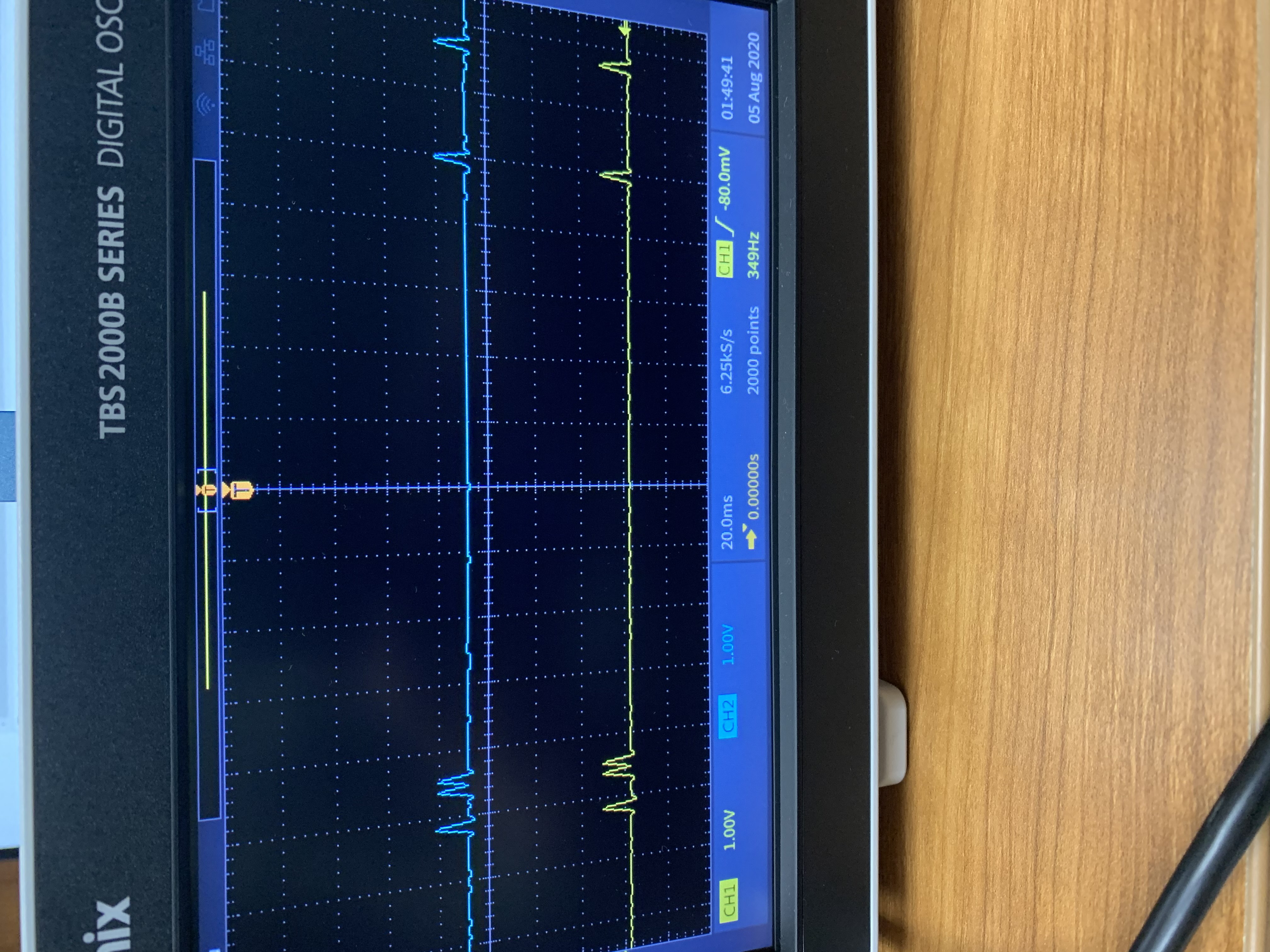
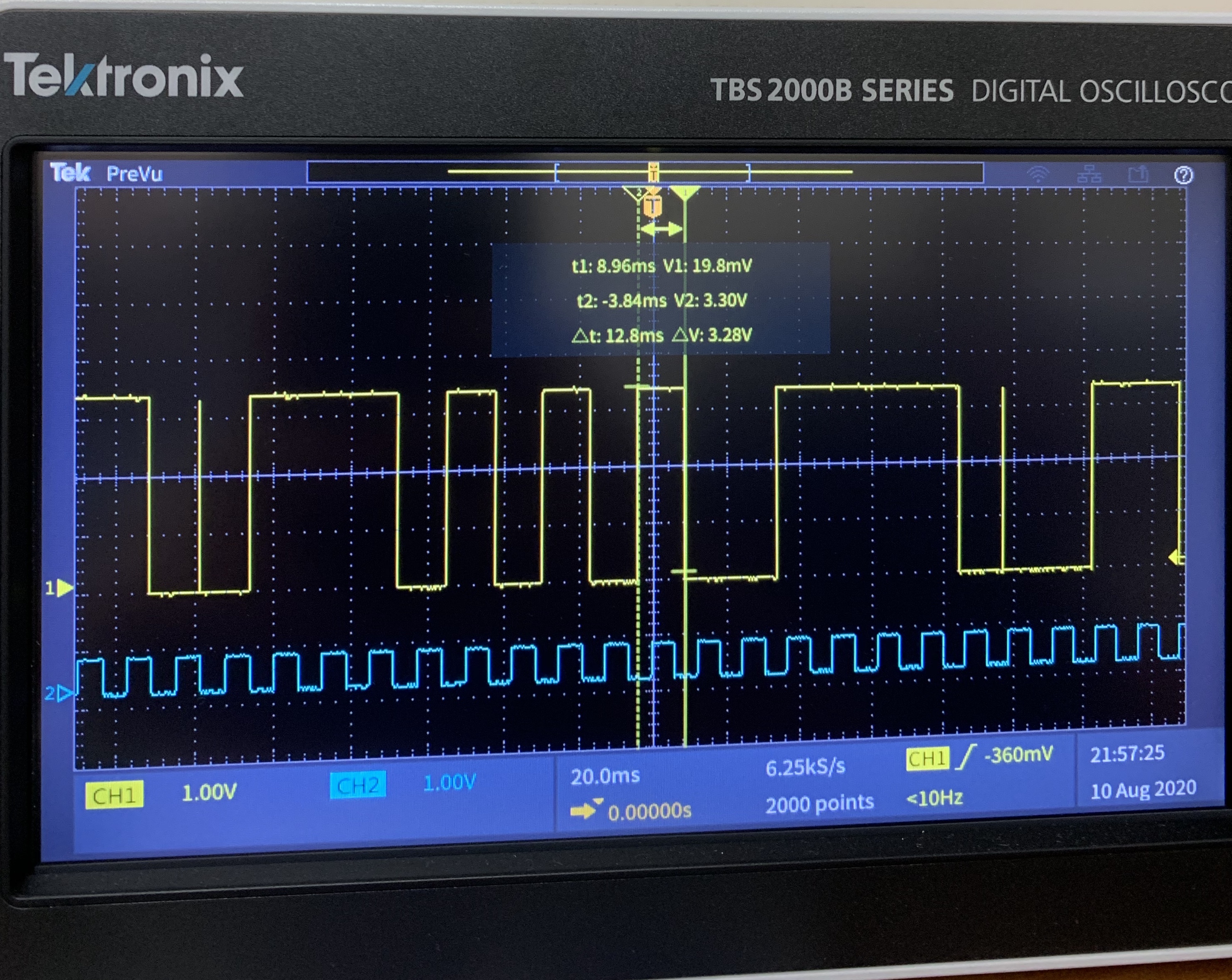
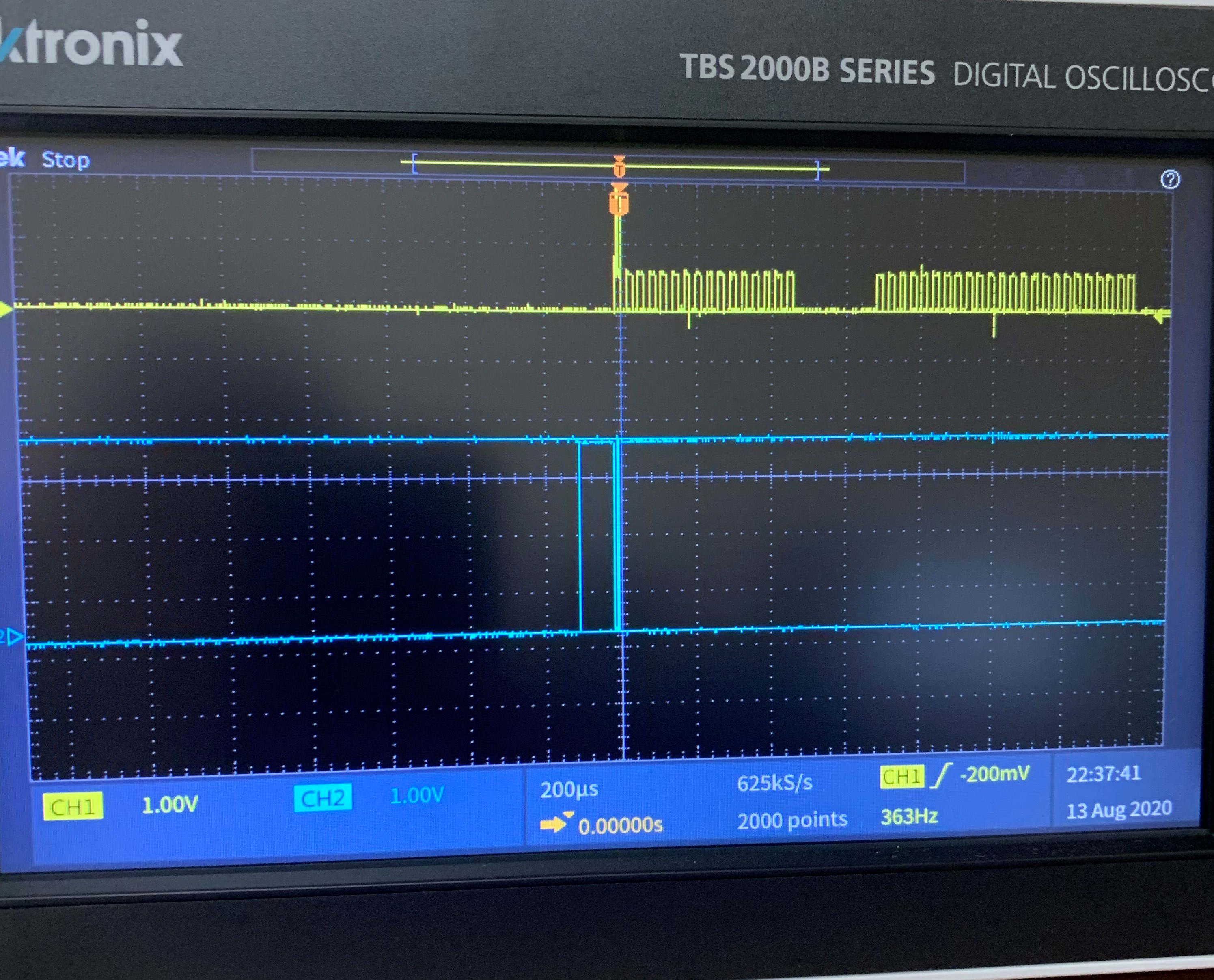
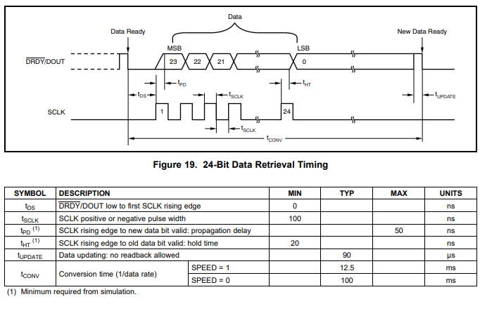
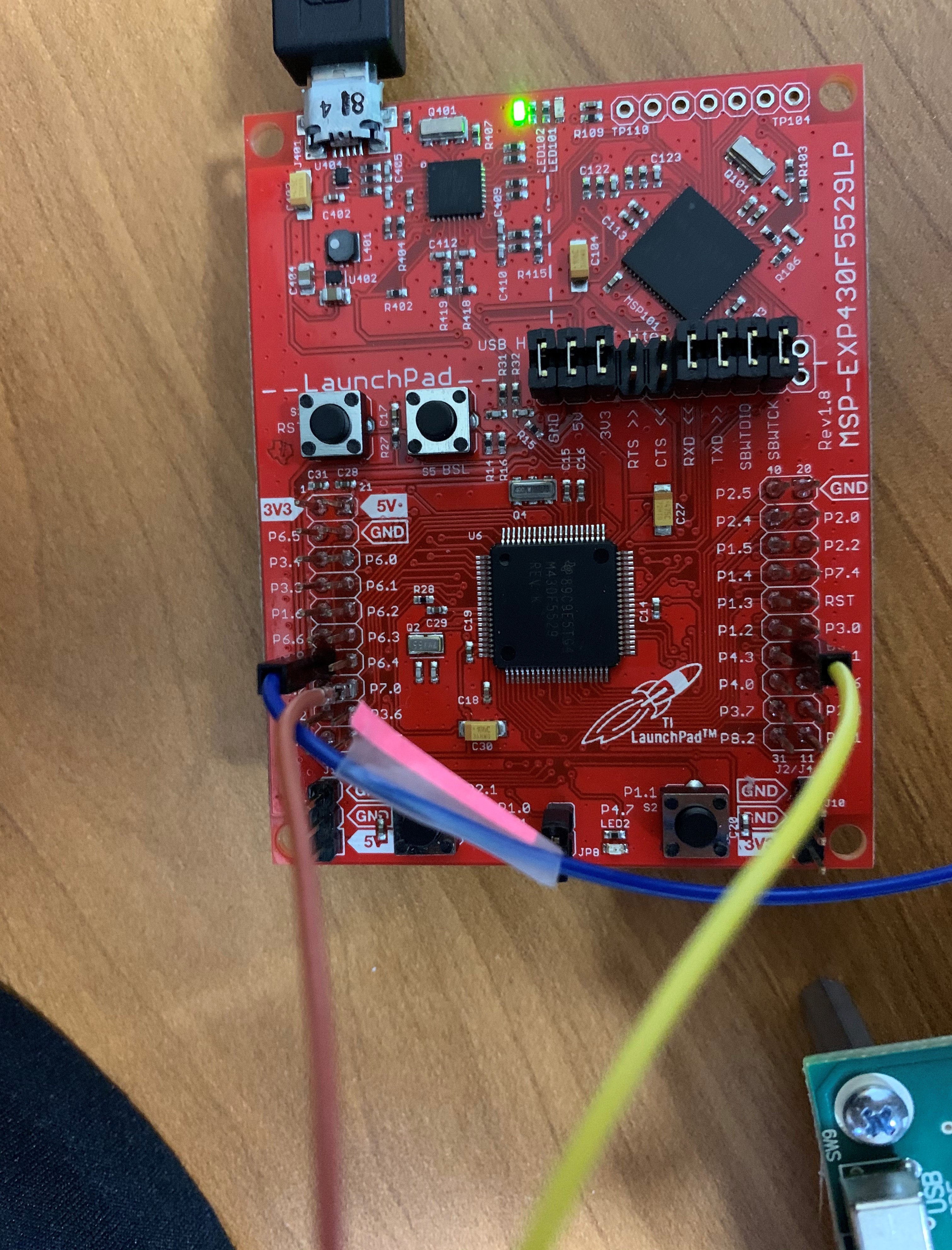
I'm trying to interface my ADS1231REF EVM with a MSP430F5529LP, but I'm not receiving any meaningful values in the receive buffer (UCB0RXBUF). I configured the SPI registers and made the proper pin connections. DOUT of the ADS1231 is connected to the MISO pin (P3.1) and P7.0 of the MSP430 and SCLK of the ADS1231 is connected to the MSP430's UCB0 clock output (P3.2). According to its datasheet, the ADS1231 is ready to transmit data when its DOUT signal goes low, so I monitor P7.0 in my code. When I connect my osciloscope to the MISO pin of the MSP430, I see the correct data being outputted from the ADS1231REF board, but the only values I receive in the receive buffer in Code Composer is similar to the following console log:

The adc_data is 3fffff.
The adc_data is 0000.
The adc_data is ffffffff.
The adc_data is 0000.
The adc_data is ffffffff.
The adc_data is fffff.
The adc_data is ffffffff.
The adc_data is 0000.
The adc_data is ffffffff.

Attached is my code. I would really appreciate any help to solve this problem.

Thank you

#include <msp430.h>
#include <stdio.h>

int32_t data1, data2, data3, signExtension, adc_data;
char sign;

void SPI_init()
{
     UCB0CTL1 |= UCSWRST;                // software reset enable
     UCB0CTL0 = UCMST + UCSYNC + UCMODE_0 + UCMSB + UCCKPL;
     UCB0CTL1 |= UCSSEL_3;               // select SMCLK

     UCB0BRW = 109;                             // 1 MHz / 109 = 9600 bps

     P3SEL = BIT0 + BIT1 + BIT2;           // configure SPI pins

     P7DIR &= ~BIT0;                              // P7.0 = DRDY, set as input
     P7OUT |= BIT0;

     UCB0CTL1 &= ~UCSWRST; //software reset disable

}

int main(void)
{
     SPI_init();             // configure SPI registers

     while (1)                    // infinite loop
     {
          while (!(P7IN & 0x01));                                     // is DRDY/DOUT low / is ADS1231 ready to Tx data?
          while (!(UCB0IFG & UCTXIFG));
          UCB0TXBUF = 0x00;                                       // transmit dummy value
          while (!(UCB0IFG & UCRXIFG));
          data1 = UCB0RXBUF;
          sign = data1 >> 7;
          if (sign) signExtension = 0xff;
          else signExtension = 0x00;
          signExtension <<= 24;
          data1 = data1 << 16;

          while (!(UCB0IFG & UCTXIFG));
          UCB0TXBUF = 0x00;
          while (!(UCB0IFG & UCRXIFG));
          data2 = UCB0RXBUF;
          data2 = data2 << 8;

          while (!(UCB0IFG & UCTXIFG));
          UCB0TXBUF = 0x00;
          while (!(UCB0IFG & UCRXIFG));
          data3 = UCB0RXBUF;

          adc_data = data1 + data2 + data3 + signExtension;
          printf("The adc_data is %04lx.\n", adc_data);

     }
}

  • it seems that in cases like this, you want to first figure out if the spi module is correctly configured and if the hardware (power, wiring, ...) is in order... and then go from there.

    the code needs some work as well.

  • Based on data sheet (SBAS414D) Fig 19, I think you need UCCKPL=0. (UCCKPH=0 looks right.)

    The section "Data Retrieval" (immediately preceding) says that DRDY/DOUT is indeterminate between reading the 3 bytes and the next DRDY event. This may mean your code is reading when there's no sample ready. The fix/workaround they suggest is to do a 25th SCK cycle; doing a single cycle isn't so easy to do, but I suspect sending another byte (8 more SCK cycles) then throwing away the result will accomplish the same purpose.

    SPI speed of 9.6kHz is pretty slow. Are you fairly certain you'll fetch everything within Tupdate? The table on p.3 indicates it can run up to 5MHz.

  • Thank you for your help.

    I set UCCKPL = 0 and changed the frequency of SCLK to be 1 MHz. I also sent a fourth byte to the UCB0TXBUF in order to get 8 more cycles of SCLK and set DRDY high. Still, I haven't had any luck.

    I also noticed that when I connect my oscilloscope to the SPI clock output pin of my MSP430, SCLK doesn't show up, so I assume the clock signal isn't being generated.

  • I based my SPI configuration code off of the examples provided by TI. I'm almost positive that my wiring connections are correct, and both the ADS1231REF board and the MSP430F5529LP are properly powered.

    What can I improve about my code?

    Thank you for your help.

  • If the SPI clock weren't running, you would have stayed stuck at the RXIFG check, so if you're seeing the printf() displays, but not seeing any SCLKs, that suggests something between the SPI unit and the wire. Stating the obvious: If the SCLKs don't reach the slave, it won't send any data.

    Your P3SEL settings looks right. Where exactly are you probing the SCLK wire?

    [Edit: Minor re-wording]

  • I can see the SCLK signal on my oscilloscope now, I'm not sure why it wasn't working before. However, I'm still receiving irrelevant values, mostly 0xff. I know for sure that the correct data from the ADS1231 is being sent to the MISO pin of the MSP430 launchpad because I can see the signal on the oscilloscope.

    Reading from the UCB0RXBUF clears the UCRXIFG flag, which is the expected result. Writing to the UCB0TXBUF sets UCRXIFG, which I'm assuming is because the clock signal is generated when the transmit buffer is written to and a character is read on the rising edge of the clock. However, I've noticed that UCTXIFG is always set, even though it should clear when the UCB0TXBUF is written to.

  • I don't have your equipment, so all I can do is guess.

    Now that you can see the signals: Do you see the DRDY/DOUT transition to 0 after the extra dummy byte? 

    The IFG transitions you describe make sense if you realize that the SPI clock is running "behind your back", so writing TXBUF in the debugger causes the byte exchange immediately. Some devices (I forget which ones) allow the debugger to disable various clocks, but I usually "just live with it".

  • The SCLK signal has been very variable for me. I've attached two pictures to further detail my issue.

    The first picture shows the SCLK signal on my oscilloscope, with a probe attached to both the ADS1231REF side of the wire and the MSP430 side. The second picture is a zoomed-in view. As you can see, the SCLK signal is not functioning as intended. What can I do to output the correct clock signal from my MSP430 launchpad?

  • It looks as though your scope is sampling at about 6ksps, which is much too slow to catch a 1MHz SCLK signal. Can you convince it to sample faster?

  • I modified my code so that SCLK runs at approximately 80 Hz in order to synchronize with the data rate of the ADS1231REF, which is 80 sps when high. To divide the 32,768 Hz ACLK signal sourced from MSP430 into an 80 Hz signal, I set UCB0BRW to 410. However, the precise prescaler to achieve 80 Hz from 32.768 kHz is 409.6. How can I achieve this 0.6? Thanks!

  • Each sample is 24 bits, so your SCLK absolute minimum at 80sps would be 24*80=1920Hz. It should actually be quite a bit faster, since you won't be able to keep the SPI busy all the time.

    To answer your question: All the USCI gives you is an integer divider, so that limits you in what bit-clock rates you can actually generate. SPI is generally not very sensitive to bit-clock speed.

  • I thought it should be 1920 Hz as well, but it seems from my oscilloscope that each bit of data is roughly 12.5 ms long, meaning only 80 bits are transferred every second.

  • Each SCLK is 1 bit, so SCLK=80Hz gives you 80 bits/second, or just over 3 samples/second. SCLK=1920Hz gives you (80*24) bits/second, or about 80 samples/second.

    More generally, I'm not clear what your goal is in running the SCLK so slowly. As the SPI master, you have total control over the bus speed, so there is rarely a reason to run the SPI much slower than the slave is capable of. SCLK=1MHz should be fine. Google tells me that your scope is capable of capturing 70MHz, so with the right settings you should be able to see even a fast SCLK. 

  • The reason why I'm running the SCLK so slowly is because I'm trying to match the clock signal with the rate at which data is being outputted from my ADS1231REF board. If I try to speed up SCLK, the data rate of the ADS1231REF remains at 80 bits per second.

  • And these are my results:

    The adc_data is -4013314.
    The adc_data is -2105438.
    The adc_data is 5592520.
    The adc_data is -1118509.
    The adc_data is -3487165.
    The adc_data is -4144919.
    The adc_data is 1118714.
    The adc_data is 7434582.
    The adc_data is -329034.
    The adc_data is 4671358.

    Why am I receiving inconsistent results, none of which matching the expected digital code for my calibration weight?

  • What SCLK speed are you using? If it's still 80Hz (or maybe even 1920Hz), I expect you're getting fragments of multiple ADC samples concatenated together.

  • The SCLK speed is at roughly 80 Hz, but I’ve tried it at different speeds and the bits per second the ADS1231REF outputs data at remains the same.

  • With SCLK=80Hz, you will not get correct results. [Ref data sheet (SBAS414D) p. 13 "Data Retrieval"] Even at 10sps, the device has 240 bits of information to give you each second, and you can only collect 80 of them.

    What other speeds did you try?

  • When I set SCLK faster (in this case to 32.768 kHz), the clock doesn't run continuously like it did at 80 Hz, but instead it pulses every so often, as you can see in the image below. How can the bits shift out if the clock only pulses during the duration of one, maybe two bits?

  • The bursty behavior of SCLK is expected. In between, your program is spinning on P7IN, waiting for DRDY. This is a good thing. As your program develops, you'll find other things to do in between DRDY signals.

    I only see a few SCLK cycles in each burst on your scope, but I'm not sure I believe that since I also see "3.12kS/s" down at the bottom, which is much too slow to see a 32kHz SCLK. Google tells me that your scope can capture 70MHz, with the appropriate settings. (Is there a knob marked "T"ime or "X" or "Horizontal"?)

    What sort of (numeric) results are you seeing? And what results are you expecting, based on what you're providing to the ADC's input?

  • There are two knobs in the "Horizontal" section. One to adjust the position and the other for the scale. I can turn the "scale" knob to increase the sampling rate.

    I've noticed that when I stop my program, there are more clock pulses than when the program is running. The expected results should be a digital code around 239880 in decimal. However, these are the results I'm receiving with a 32,768 Hz SCLK:

    The adc_data is -1.
    The adc_data is 0.
    The adc_data is -1.
    The adc_data is -2097153.
    The adc_data is 0.
    The adc_data is -1.
    The adc_data is -1.
    The adc_data is -1.
    The adc_data is 0.
    The adc_data is -1.
    The adc_data is 0.
    The adc_data is 8388607.
    The adc_data is 0.
    The adc_data is -1.

  • 1) Data sheet p. 13 says to "Avoid data retrieval during the update period (Tupdate)", without saying what the consequences are. You wait for DRDY (P7.0) to go high, then start the transaction. This actually starts the transfer within Tupdate. After the "while (!(P2IN&BIT0))" add another loop "while (P2IN & BIT0)" to wait for DRDY to go low (about 90 usec).

    2) With the Horizontal axis expanded, do you see DRDY go low after sending the extra "dummy" byte? What we're doing isn't strictly according to the data sheet; I still expect it does the right thing, but it would be good to see it.

    My spreadsheet says that code 239880 corresponds to about 559 uV (micro-volts). Does that sound about right? [Ref REF data sheet (SBAU175A) Formula (3), ADS1231 data sheet (SBAS414D) Table 3]

  • I thought by transmitting a fourth value to UCB0TXBUF and generating a 25th clock pulse, DRDY is set high and, and then the program ("while(!(P7IN & BIT0))") polls P7.0 until it goes low and new data is ready to be outputted. If this is the case, what is the purpose of adding a second loop?

    From what I can tell, DRDY is not forced high after sending the extra "dummy" byte. It's hard to tell which clock pulse aligns with which of the four bytes being transmitted, but there is no point in the oscilloscope reading where DRDY remains high. As you can see, the clock is not generated for long enough at one time, and the same bit might be picked up at two subsequent rising edges. This is why I figured I should set SCLK to 80 Hz, so at each rising edge there is a new bit ready to be transmitted.

  • Yamen,

    I am moving this thread to the data converters forum where someone should be able to help clarify the correct ADS operation.  There is also an EVM for the ADS1231 with MSP430, but I don't see the example source code.  

    https://www.ti.com/tool/ADS1231REF

  • I was mistaken. You are correct that the 25th clock forces DRDY high, not low (per Fig 20). In that case, you need to reverse the test you have so that it will end when the pin goes low:

    > while (P7IN & BIT0); // spin as long as P7.0 (DRDY) stays high

    This (still) supposes that the 8-extra-clocks works as expected. I still don't quite understand why you can't get more horizontal resolution from your scope. 100ms is a very long time for a 32kHz clock.

    Eddie raises a good question: What board are you using?

    [Edit: Fixed typo]

  • I'm a little confused. Why do we need to test whether DRDY goes high? In the datasheet, it explains that the signal goes high until new data is ready. Then, DRDY goes low to signify that new data is ready. As long as we poll for DRDY going low, and we see that it does, we can transmit a dummy value to receive the first byte in UCB0RXBUF.

    I'm using the ADS1231REF board that Eddie mentions in his reply.

    I can get more horizontal resolution from my scope, but the signal becomes very choppy and it's difficult to pause the run at the right place, but I managed to get a picture. As you can see, SCLK goes by so quickly that it picks up data from only one bit.

  • 1) Your original loop was constructed to keep looping "while" P7.0 was low (=0) and break out when P7.0 went high (=1). The effect is to wait for P7.0 to go high. I suggested reversing the logic so it breaks out of the while loop when P7.0 goes low.

    2) The scope trace is a little hard to read, CH2 seems to have multiple traces, maybe some kind of persistence. (On my Rigol scope I get rid of this by stepping the Horizontal knob one step either direction, then back where it was. I guess it forces the scope to re-draw the screen or something.) But it looks (sort of) like you're running SCLK while DRDY is high, which would match with the code (see (1)).

    What concerns me more is that the SCLK (CH1) amplitude is only around 0.5V. I suppose this could be a scope (aliasing) artifact, but those aren't usually so consistent.

    Looking at the ADS1231REF schematics, I don't see a way to switch off the MSP430F449 chip, nor to disconnect SCLK/DOUT from it. It's possible that the on-board MSP430 is fighting with you (bus contention) for SCLK. Did you modify the REF board? Or is there some switch or something that I'm not seeing?

    [Edit: Here's a quick experiment: Press and hold down the RST button (SW6) on the REF board while you run your program, and see if the CH1 trace changes (maybe up to 3V). Holding the F449 in reset will force it to let go of SCLK.]

  • Doesn't my original loop wait for P7.0 to go low, because once the pin's low state is AND'ed with BIT0, the result is a 0, which is then inversed to become a 1, and the loop is fulfilled?

    According to the timing diagram on p.13 of ADS1231's datasheet, the total time for all 24 bits of data to output (t_conv) should be 12.5 ms when SPEED is high, which I have configured on my ADS1231REF board. However, my oscilloscope shows the signal functioning otherwise. Why is one bit of data roughly 12.5 ms long when all 24 bits should be outputted in that duration? How can I speed up my board's data output?

    I didn't modify the REF board, and I tried to hold down the RST button while I ran my progam, with no luck. By the way, my MCU is the MSP430F5529, not the MSP430F449, if that helps.

  • I agree with you about the while() as long as "fulfilled" means "still true, so it keeps looping". So as long as P7.0 is low, it will keep looping. This is how C works.

    It wasn't until Eddie mentioned it that I noticed that there is an MSP430F449 on the board, and since that's not the device you've been describing I started to suspect that the on-board MCU was causing trouble for you. One suspicion is that it's keeping the ADC from seeing your SCLKs. I don't see a header for DOUT/SCLK; how are you connecting to them? TP6 and TP9? Maybe a photo of your setup would be useful.

    I was guessing that the "bits" you were seeing were actually DRDY cycles in the absence of anything being read (no SCLKs) [Ref data sheet Fig 21]. As you say, I would expect those to be half that long. Or I suppose it could be an aliasing effect from your scope's slow sample rate.

    When you held down the RST, was that SW6, or SW1 ("USB reset")? You need to use SW6.

  • I understand what you mean. So I should have "while (P7IN & BIT0)" first, which waits for DRDY to go low (meaning new data is ready) before exiting the loop. Then, I should send a dummy value to the transmit buffer to generate the first rising edge of SCLK, at which the first bit will begin to transmit. Is this correct?

    Here's a few photos of my setup. The ADS1231REF board is connected at the load cell header to a wooden slab on which four 50 kg load cells are attached to each corner.

    The button I held down to reset the ADS1231REF board was SW6.

  • Looking at the LCD screen, it really looks like the on-board MCU is running, and probably driving SCLK low to create a bus-conflict with your SCLK.

    I don't have an ADS1231REF, all I can do is read the schematics. Maybe Eddie is right, and we should ask the Data Converters people how to do this.

  • Thank you for your help! I hope we can get this solved.

  • This conversation continues on the following thread:

    https://e2e.ti.com/support/data-converters/f/73/t/933142

**Attention** This is a public forum