Part Number: ADS54J54EVM
Other Parts Discussed in Thread: ADS54J54, LMK04828
I have the following two evaluation boards.
- ADC Board: ADS54J54EVM Rev C
- FPGA Board: TSW14J56 Rev E
I'm following the instructions from Section 3.3.3 and 3.3.4 from SLAU616A. However, when I attempt a capture, I receive a Read DDR to file TIMED_OUT_ERROR message.
Here is the sequence of steps I followed:
Connect ADC Board to FPGA Board
Connect 5V supply to ADC Board and power on (Using provide PSU)
Connect 5V supply to FPGA Board and power on (SW6 to ON) (PSU rated to 20A)
Connect ADC Board USB cable to PC
Connect FPGA Board USB cable to PC
Connect 5V supply to ADC Board and power on (Using provide PSU)
Connect 5V supply to FPGA Board and power on (SW6 to ON) (PSU rated to 20A)
Connect ADC Board USB cable to PC
Connect FPGA Board USB cable to PC
Connect a 10MHz sinusoid (50mVpp) to J22 (Chan D +)
Start ADS54J54 EVM GUI (Build Date 12/18/14, Prelim devbug)
Check for Green LED Icon on USB Status
On ADS54J54 -> ADC Configuration Tab check 'Device Reset' checkbox
On LMK04828 -> PLL1 Configuration Tab check 'RESET' checkbox
On Low Level View Tab, click 'Load Config' button
Select ADS54J54_500M_442.cfg
Select ADS54J54_500M_442.cfg
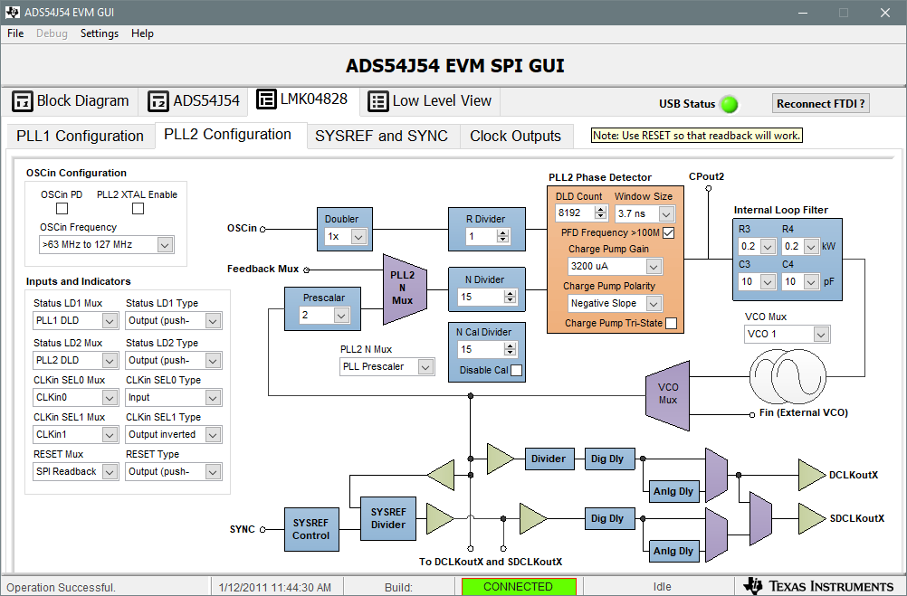
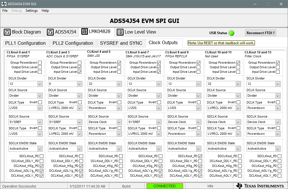
The following 6 screen shots show the GUI state after the config file has been loaded



Checked ADC Board LEDS:
- D1 LMK Locked is illuminated
- D4 PLL2 Locked is illuminated
- D1 LMK Locked is illuminated
- D4 PLL2 Locked is illuminated
- D3 JESD_SYNC is illuminated, but it is very faint
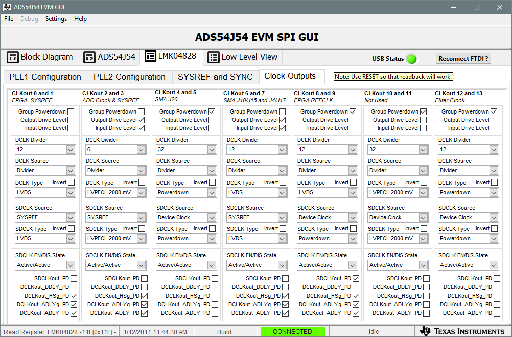
Disabled Group Powerdown for CLKOut 6 and 7
Set CLKOut 7 to LVDS
Set CLKOut 7 to LVDS
Confirmed 250 MHZ on SMA J10 (CLKOut 6) - This should be the same as JESD Core Clock going to FPGA
Confirmed 1.5625 MHZ on SMA J17 (CLKOut 7) - This should be the same as JESD Core SYSREF going to FPGA
Confirmed 1.5625 MHZ on SMA J17 (CLKOut 7) - This should be the same as JESD Core SYSREF going to FPGA
The screen shot below shows the change in settings to allow 'copies' of the JESD Clock and SYSREF to be observed.
Start High Speed Data Converter Pro v4.90
- Dll version 0.1
- Firmware version 0.2
- No Patch Applied
The software hangs for 150 seconds. The grey and black progress bars just scroll.
I suspect some kind of network access that is slowly timing out.
I suspect some kind of network access that is slowly timing out.
The Select Board Dialog appears. Select the board from the list and click OK
The following dialog appears:
'No firmware. Please select a device to load firmware into the board'
Click OK
'No firmware. Please select a device to load firmware into the board'
Click OK
Click the green arrow next to Select ADC
Select 'ADS54J54_LMF_442' from list
Select 'ADS54J54_LMF_442' from list
The following dialog appears:
'Do you want to update the Firmware for the ADC?'
Click Yes
'Do you want to update the Firmware for the ADC?'
Click Yes
These are the states of the FPGA board LEDs
D28 CONFIG_DONE is illuminated
D8 MEM FAIL~ is illuminated
D7 MEM SUCCESS~ is off
D6 MEM INIT DONEE~ is off
D4 RX CLK is off
D3 RX SYNS~ is illuminated
D2 TX CLK is off
D1 TX SYNS~ is illuminated
D28 CONFIG_DONE is illuminated
D8 MEM FAIL~ is illuminated
D7 MEM SUCCESS~ is off
D6 MEM INIT DONEE~ is off
D4 RX CLK is off
D3 RX SYNS~ is illuminated
D2 TX CLK is off
D1 TX SYNS~ is illuminated
ADC Board LED D3 (JESD_SYNC) is still faintly illuminated
Enter 250M in the ADC Output Data Rate Box
The following dialog appears:
'New lane rate is 5G due to ADC Output Data Rate change'
'JESD reference clock from device EVM to TSW14J56revD needs to be set at 250M
Click OK
'New lane rate is 5G due to ADC Output Data Rate change'
'JESD reference clock from device EVM to TSW14J56revD needs to be set at 250M
Click OK
Click Capture
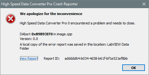
Get Read DDR to file TIMED_OUT_ERROR message as shown in the screen shot below.

Here's some things I've tried/observed.
- All the blue LEDS on the FPGA board are illuminated
- The error message states D4 LED should be blinking. I'm assuming this is D4 on the FPGA board (RX CLK); I've only seen this on or off, not blinking
- The HSDC Pro software mentions RevD of TSW14J56, I have Rev E.
- I've tried other USB ports, but this hasn't helped
- The LMK04828 is configured for LVPECL on the ADS54J54 SYSREF input. The ADS54J54 datasheet states these are LVDS inputs

Hope someone can help.
Thanks
Andy