Hello
i am able to get the ACK if write a slave address and any other commands from the ADS112C04. every command which i wrote.
steps I am following :
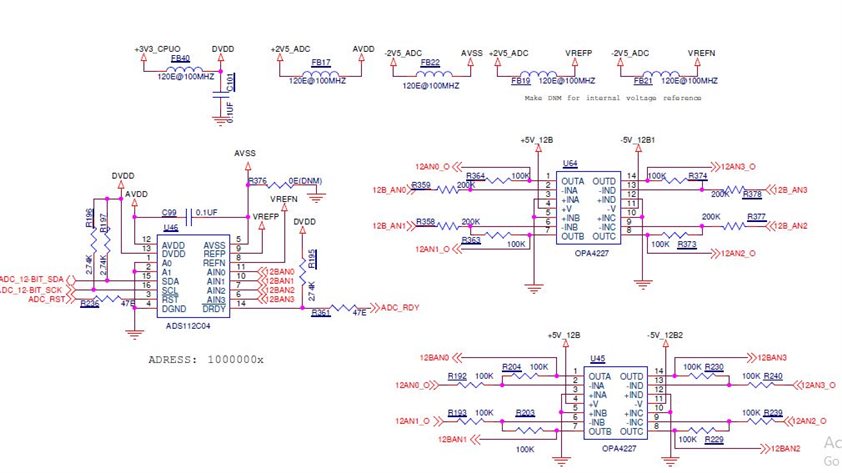
1.reset the ADS112C04 by issuing the below command
<S>0x80 0x06 <P>
2.i am trying in the single-shot mode it is set as default.
3. i am writing to ANI0 by follows
<S> 0x80 0x40 0x81 <P> // WREG command to set the mux
<S> 0x80 0x08 <P> // ADC START/SYNC conversion command
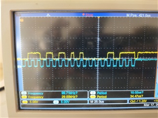
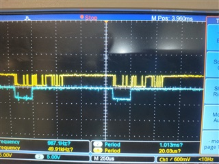
Monitor DRDY and wait for DRDY to transition from high to low
<S> 0x80 0x10 <Sr> 0x81 {MSB byte} {LSB Byte} <P> // RDATA command and data returned from ADC
4.after read command i am sending for AIN1
<S> 0x80 0x40 0x91 <P> // WREG command to set the mux
<S> 0x80 0x08 <P> // ADC START/SYNC conversion command
Monitor DRDY and wait for DRDY to transition from high to low
5.after read command i am sending for AIN2
<S> 0x80 0x40 0xa1 <P> // WREG command to set the mux
<S> 0x80 0x08 <P> // ADC START/SYNC conversion command
Monitor DRDY and wait for DRDY to transition from high to low
6.after read command i am sending for AIN3
<S> 0x80 0x40 0xb1 <P> // WREG command to set the mux
<S> 0x80 0x08 <P> // ADC START/SYNC conversion command
Monitor DRDY and wait for DRDY to transition from high to low
after last channel again i am repeating the step 3 .
But for me DRDY pin is not moving to High to LOW . after 2 or 3 sec's and the read data is alwasy high if i apply 0 v also.
Please help me regards this issue?
Regards,
Naresh reddy


 Hello Bob B..