This thread has been locked.

If you have a related question, please click the "Ask a related question" button in the top right corner. The newly created question will be automatically linked to this question.

ADC12J4000 HAS STRONG INTERLEAVED SPUR AT ¼ OF SAMPLING FREQUENCY IN DDC MODE

Other Parts Discussed in Thread: ADC12J4000, ADC12J4000EVM

e2e,

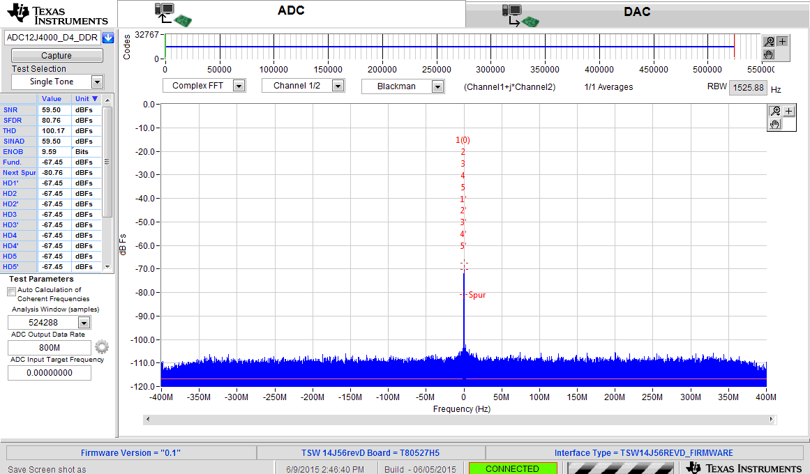
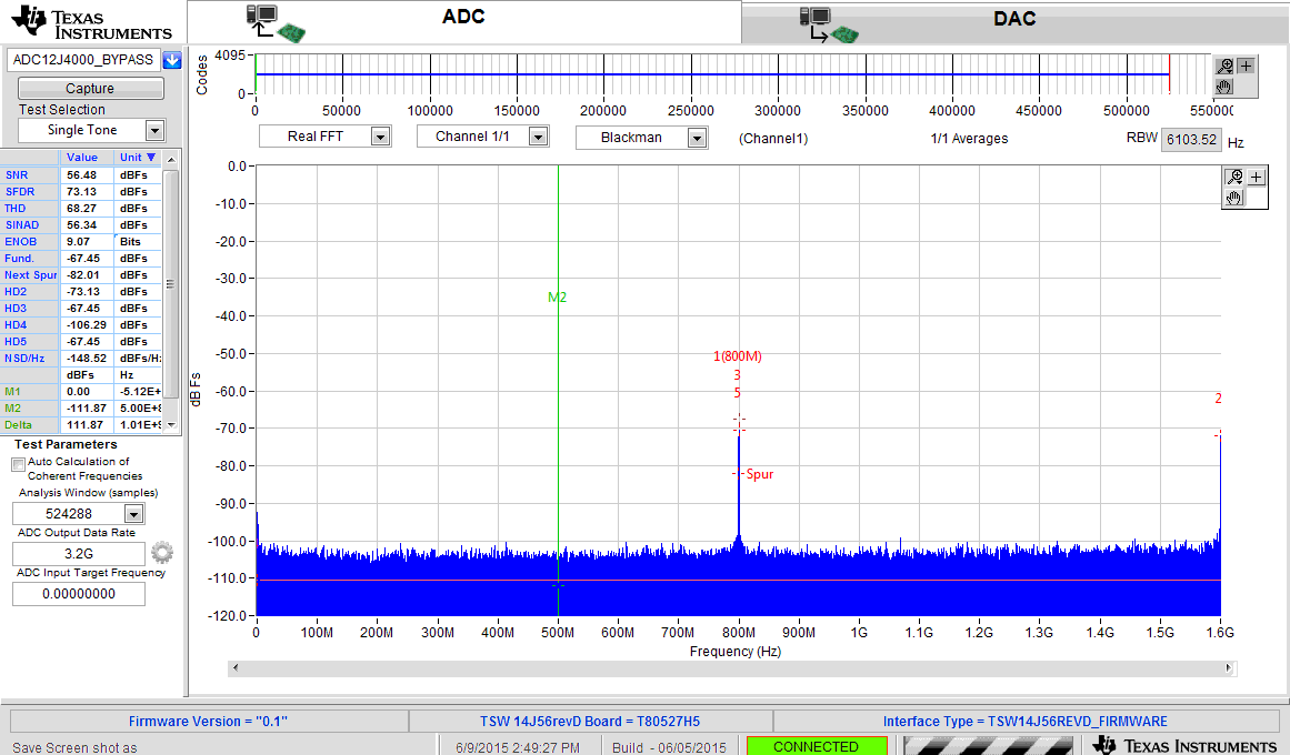
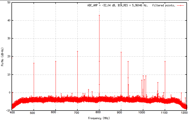
We have a customer that has noticed that the ADC12J4000 has a strong interleave spur at ¼ of the sampling frequency in DDC mode. In normal mode, the interleave spur can be reduced significant by enabling the timing calibration mode. Attached plot please find the acquired ADC spectrum from white noise input.


The test setup:

3.2GHz sampling rate

Decimation = 4

P54 = 1 (L = 4)

NCO = -800MHz (2.4GHz)

DDC gain off

Please explain the reason the DDC adds this spur.

Thanks for your help.

Regards,

John Wiemeyer

adc12j4000.txt
//---- Dumping ADC12J4000 Registers ---------
Addr  	Data 	Name


ADC12J4000 #1

0x000 	0x3C	Cfg_A
0x001 	0x00	Cfg_B
0x002 	0x00	Device configuration
0x003 	0x03	Chip type = 0x03
0x006 	0x03	Chip version = 0x03
0x00C 	0x51	Vender ID = 0x51
0x00D 	0x04	Vender ID = 0x04
0x010 	0x00	SPI configuration
0x021 	0x00	Power on reset
0x022 	0x40	I/O gain 0
0x023 	0x00	I/O gain 1
0x025 	0x40	I/O offset 0
0x026 	0x00	I/O offset 1
0x030 	0xC0	Clock generator control 0
0x031 	0xC7	Clock generator status
0x032 	0x80	Clock generator control 2
0x033 	0xC3	Analog miscellaneous
0x034 	0x2F	Input clamp enable
0x040 	0x04	Serializer configuration
0x050 	0x06	Calibration configuration 0
0x051 	0xF4	Calibration configuration 1
0x057 	0x10	Calibration background control
0x058 	0x00	ADC pattern and over-range enable
0x05A 	0x00	Calibration vector
0x05B 	0x0F	Calibration status
0x066 	0x03	Timing calibration
0x200 	0x32	Digital down-converter (DDC) control
0x201 	0x7F	JESD204B control 1
0x202 	0x80	JESD204B control 2
0x203 	0x00	JESD204B Device ID
0x204 	0x00	JESD204B control 3
0x205 	0x7C	JESD204B status [6] link up; [5]: sync~ deasserted; [4] realigned; [3] aligned; [2] pll_locked
0x206 	0xF2	Over-range control 0
0x207 	0xAB	Over-range control 1
0x208 	0x00	Over-range period
0x20C 	0x01	DDC configuration preset mode
0x20D 	0x00	DDC configuration preset select
0x20E 	0x00	NCO_RDIV[7:0]
0x20F 	0x00	NCO_RDIV[15:8]
0x210 	0x00	 NCO_FREQ_0[7:0]
0x211 	0x00	 NCO_FREQ_0[15:8]
0x212 	0x00	 NCO_FREQ_0[23:16]
0x213 	0xE0	 NCO_FREQ_0[31:24]
0x214 	0x00	NCO_PHASE_0[7:0]
0x215 	0x00	NCO_PHASE_0[15:8]
0x216 	0xFF	  DDC_DLY_0
0x218 	0x00	 NCO_FREQ_1[7:0]
0x219 	0x00	 NCO_FREQ_1[15:8]
0x21A 	0x00	 NCO_FREQ_1[23:16]
0x21B 	0x80	 NCO_FREQ_1[31:24]
0x21C 	0x00	NCO_PHASE_1[7:0]
0x21D 	0x00	NCO_PHASE_1[15:8]
0x21E 	0xFF	  DDC_DLY_1
0x220 	0x00	 NCO_FREQ_2[7:0]
0x221 	0x00	 NCO_FREQ_2[15:8]
0x222 	0x00	 NCO_FREQ_2[23:16]
0x223 	0x40	 NCO_FREQ_2[31:24]
0x224 	0x00	NCO_PHASE_2[7:0]
0x225 	0x00	NCO_PHASE_2[15:8]
0x226 	0xFF	  DDC_DLY_2
0x228 	0x00	 NCO_FREQ_3[7:0]
0x229 	0x00	 NCO_FREQ_3[15:8]
0x22A 	0x00	 NCO_FREQ_3[23:16]
0x22B 	0x20	 NCO_FREQ_3[31:24]
0x22C 	0x00	NCO_PHASE_3[7:0]
0x22D 	0x00	NCO_PHASE_3[15:8]
0x22E 	0xFF	  DDC_DLY_3
0x230 	0x00	 NCO_FREQ_4[7:0]
0x231 	0x00	 NCO_FREQ_4[15:8]
0x232 	0x00	 NCO_FREQ_4[23:16]
0x233 	0x10	 NCO_FREQ_4[31:24]
0x234 	0x00	NCO_PHASE_4[7:0]
0x235 	0x00	NCO_PHASE_4[15:8]
0x236 	0xFF	  DDC_DLY_4
0x238 	0x00	 NCO_FREQ_5[7:0]
0x239 	0x00	 NCO_FREQ_5[15:8]
0x23A 	0x00	 NCO_FREQ_5[23:16]
0x23B 	0x08	 NCO_FREQ_5[31:24]
0x23C 	0x00	NCO_PHASE_5[7:0]
0x23D 	0x00	NCO_PHASE_5[15:8]
0x23E 	0xFF	  DDC_DLY_5
0x240 	0x00	 NCO_FREQ_6[31:24]
0x241 	0x00	 NCO_FREQ_6[23:16]
0x242 	0x00	 NCO_FREQ_6[15:8]
0x243 	0x04	 NCO_FREQ_6[7:0]
0x244 	0x00	NCO_PHASE_6[7:0]
0x245 	0x00	NCO_PHASE_6[15:8]
0x246 	0xFF	  DDC_DLY_6
0x248 	0x00	 NCO_FREQ_7[31:24]
0x249 	0x00	 NCO_FREQ_7[23:16]
0x24A 	0x00	 NCO_FREQ_7[15:8]
0x24B 	0x00	 NCO_FREQ_7[7:0]
0x24C 	0x00	NCO_PHASE_7[7:0]
0x24D 	0x00	NCO_PHASE_7[15:8]
0x24E 	0xFF	  DDC_DLY_7


ADC12J4000 #2

0x000 	0x3C	Cfg_A
0x001 	0x00	Cfg_B
0x002 	0x00	Device configuration
0x003 	0x03	Chip type = 0x03
0x006 	0x03	Chip version = 0x03
0x00C 	0x51	Vender ID = 0x51
0x00D 	0x04	Vender ID = 0x04
0x010 	0x00	SPI configuration
0x021 	0x00	Power on reset
0x022 	0x40	I/O gain 0
0x023 	0x00	I/O gain 1
0x025 	0x40	I/O offset 0
0x026 	0x00	I/O offset 1
0x030 	0xC0	Clock generator control 0
0x031 	0xC7	Clock generator status
0x032 	0x80	Clock generator control 2
0x033 	0xC3	Analog miscellaneous
0x034 	0x2F	Input clamp enable
0x040 	0x04	Serializer configuration
0x050 	0x06	Calibration configuration 0
0x051 	0xF4	Calibration configuration 1
0x057 	0x10	Calibration background control
0x058 	0x00	ADC pattern and over-range enable
0x05A 	0xC9	Calibration vector
0x05B 	0x0B	Calibration status
0x066 	0x03	Timing calibration
0x200 	0x32	Digital down-converter (DDC) control
0x201 	0x7F	JESD204B control 1
0x202 	0x80	JESD204B control 2
0x203 	0x00	JESD204B Device ID
0x204 	0x00	JESD204B control 3
0x205 	0x7C	JESD204B status [6] link up; [5]: sync~ deasserted; [4] realigned; [3] aligned; [2] pll_locked
0x206 	0xF2	Over-range control 0
0x207 	0xAB	Over-range control 1
0x208 	0x00	Over-range period
0x20C 	0x01	DDC configuration preset mode
0x20D 	0x00	DDC configuration preset select
0x20E 	0x00	NCO_RDIV[7:0]
0x20F 	0x00	NCO_RDIV[15:8]
0x210 	0x00	 NCO_FREQ_0[7:0]
0x211 	0x00	 NCO_FREQ_0[15:8]
0x212 	0x00	 NCO_FREQ_0[23:16]
0x213 	0xE0	 NCO_FREQ_0[31:24]
0x214 	0x00	NCO_PHASE_0[7:0]
0x215 	0x00	NCO_PHASE_0[15:8]
0x216 	0xFF	  DDC_DLY_0
0x218 	0x00	 NCO_FREQ_1[7:0]
0x219 	0x00	 NCO_FREQ_1[15:8]
0x21A 	0x00	 NCO_FREQ_1[23:16]
0x21B 	0x80	 NCO_FREQ_1[31:24]
0x21C 	0x00	NCO_PHASE_1[7:0]
0x21D 	0x00	NCO_PHASE_1[15:8]
0x21E 	0xFF	  DDC_DLY_1
0x220 	0x00	 NCO_FREQ_2[7:0]
0x221 	0x00	 NCO_FREQ_2[15:8]
0x222 	0x00	 NCO_FREQ_2[23:16]
0x223 	0x40	 NCO_FREQ_2[31:24]
0x224 	0x00	NCO_PHASE_2[7:0]
0x225 	0x00	NCO_PHASE_2[15:8]
0x226 	0xFF	  DDC_DLY_2
0x228 	0x00	 NCO_FREQ_3[7:0]
0x229 	0x00	 NCO_FREQ_3[15:8]
0x22A 	0x00	 NCO_FREQ_3[23:16]
0x22B 	0x20	 NCO_FREQ_3[31:24]
0x22C 	0x00	NCO_PHASE_3[7:0]
0x22D 	0x00	NCO_PHASE_3[15:8]
0x22E 	0xFF	  DDC_DLY_3
0x230 	0x00	 NCO_FREQ_4[7:0]
0x231 	0x00	 NCO_FREQ_4[15:8]
0x232 	0x00	 NCO_FREQ_4[23:16]
0x233 	0x10	 NCO_FREQ_4[31:24]
0x234 	0x00	NCO_PHASE_4[7:0]
0x235 	0x00	NCO_PHASE_4[15:8]
0x236 	0xFF	  DDC_DLY_4
0x238 	0x00	 NCO_FREQ_5[7:0]
0x239 	0x00	 NCO_FREQ_5[15:8]
0x23A 	0x00	 NCO_FREQ_5[23:16]
0x23B 	0x08	 NCO_FREQ_5[31:24]
0x23C 	0x00	NCO_PHASE_5[7:0]
0x23D 	0x00	NCO_PHASE_5[15:8]
0x23E 	0xFF	  DDC_DLY_5
0x240 	0x00	 NCO_FREQ_6[31:24]
0x241 	0x00	 NCO_FREQ_6[23:16]
0x242 	0x00	 NCO_FREQ_6[15:8]
0x243 	0x04	 NCO_FREQ_6[7:0]
0x244 	0x00	NCO_PHASE_6[7:0]
0x245 	0x00	NCO_PHASE_6[15:8]
0x246 	0xFF	  DDC_DLY_6
0x248 	0x00	 NCO_FREQ_7[31:24]
0x249 	0x00	 NCO_FREQ_7[23:16]
0x24A 	0x00	 NCO_FREQ_7[15:8]
0x24B 	0x00	 NCO_FREQ_7[7:0]
0x24C 	0x00	NCO_PHASE_7[7:0]
0x24D 	0x00	NCO_PHASE_7[15:8]
0x24E 	0xFF	  DDC_DLY_7


  • Hi John

    The size of the fixed frequency interleaving spur (not dependent on the input signal frequency) at Fs/4 shouldn't change significantly between DDC Bypass mode (no decimation) and the Decimate by 4 mode. I gathered some data at 3.2GSPS in both modes for comparison. See below:

    1) Decimate by 4 mode - Fnco = -800 (2400) MHz - Spur is at approximately -67dBFS.

    2) DDC Bypass mode - Spur is again at approximately -67dBFS.

    Is the customer plot with a signal applied? If so can you get them to re-collect data with no input signal so the fixed frequency spur at Fs/4 is the only peak visible?

    Best regards,

    Jim B

  • Hi Jim,

    Thanks for your reply. You mention that the fixed frequency at fs/4 should not change significantly between DDC Bypass mode (no decimation) and the Decimate by 4 mode. We agree. We think there is some configuration that needs to be done in the ADC12J4000 that isn't being done. Can you look into this for us. Concerning having the customer take more data, I can certainly do this. We are not sure how to implement no input signal. I don't think you mean a floating input. How would you recommend implementing no input?

    Thanks for your help.
    Regards,
    John Wiemeyer
  • Hi John

    Is the customer using our evaluation tools (ADC12J4000EVM plus TSW14J56EVM) or their own hardware?

    If their own hardware, what FPGA are they using and did they base their design on the TI JESD204B firmware examples or from scratch using the FPGA vendor IP?

    On the ADC12J4000EVM the default configuration has the input signal applied to a single SMA connector. In this case the input can be left open (floating) or a 50 ohm termination can be applied to this port for slightly lower noise.

    If they have their own hardware they need to set the ADC inputs to 0V differential and at the center of the common mode range. If they are AC coupling to the ADC inputs they should be able to just terminate the input to the driving circuitry and the differential voltage will stabilize at 0V and the common mode will be biased by the internal ADC input termination connections.

    If they're using their own hardware, please send me the details of what configuration register settings they are writing for the two different modes they are using (DDC Bypass and Decimate by 4). I can check to make sure everthing necessary is there, and nothing extra or erroneous is being set.

    Best regards,

    Jim B

  • adc12j4000_ddc_bypass.txt
    const reg_with_name_t adc12j4000_reg[] =
    {
    	{ 0x0000, 3, 0x3c, 0x3c, "Cfg_A"},
    	{ 0x0001, 1, 0x00, 0x00, "Cfg_B"},
    	{ 0x0002, 3, 0x00, 0x00, "Device configuration"},
    	{ 0x0003, 1, 0x03, 0x03, "Chip type = 0x03"},
    	{ 0x0006, 1, 0x03, 0x03, "Chip version = 0x03"},
    	{ 0x000C, 1, 0x51, 0x51, "Vender ID = 0x51"},
    	{ 0x000D, 1, 0x04, 0x04, "Vender ID = 0x04"},
    	                          
    	{ 0x0010, 3, 0x00, 0x00, "SPI configuration"},
    	                          
    	{ 0x0021, 3, 0x00, 0x00, "Power on reset"},
    	{ 0x0022, 3, 0x40, 0x40, "I/O gain 0"},
    	{ 0x0023, 3, 0x00, 0x00, "I/O gain 1"},
    	{ 0x0025, 3, 0x40, 0x40, "I/O offset 0"},
    	{ 0x0026, 3, 0x00, 0x00, "I/O offset 1"},
    	                          
    	{ 0x0030, 3, 0xC0, 0xC0, "Clock generator control 0"},
    	{ 0x0031, 1, 0x07, 0x07, "Clock generator status"},
    	{ 0x0032, 3, 0x80, 0x80, "Clock generator control 2"},
    	{ 0x0033, 3, 0xC3, 0xC3, "Analog miscellaneous"},
    	{ 0x0034, 3, 0x2F, 0x2F, "Input clamp enable"},
    	                          
    	{ 0x0040, 3, 0x04, 0x04, "Serializer configuration"},
    	                          
    	{ 0x0050, 3, 0x06, 0x06, "Calibration configuration 0"},
    	{ 0x0051, 3, 0xF4, 0xF4, "Calibration configuration 1"},
    	{ 0x0057, 3, 0x10, 0x10, "Calibration background control"},
    	{ 0x0058, 3, 0x00, 0x00, "ADC pattern and over-range enable"},
    	{ 0x005A, 3, 0x00, 0x00, "Calibration vector"},
    	{ 0x005B, 1, 0x00, 0x00, "Calibration status"},
    	{ 0x0066, 3, 0x03, 0x02, "Timing calibration"},
    	                          
    	{ 0x0200, 3, 0x30, 0x10, "Digital down-converter (DDC) control"}, // change: output sample format = 2's complement for bypass mode
    	{ 0x0201, 3, 0x17, 0x0F, "JESD204B control 1"},	// change k=6
    	{ 0x0202, 3, 0x00, 0x00, "JESD204B control 2"},
    	{ 0x0203, 3, 0x00, 0x00, "JESD204B Device ID"},
    	{ 0x0204, 3, 0x00, 0x00, "JESD204B control 3"},
    	{ 0x0205, 1, 0x00, 0x00, "JESD204B status [6] link up; [5]: sync~ deasserted; [4] realigned; [3] aligned; [2] pll_locked"},
    	{ 0x0206, 3, 0xF2, 0xF2, "Over-range control 0"},
    	{ 0x0207, 3, 0xAB, 0xAB, "Over-range control 1"},
    	{ 0x0208, 3, 0x00, 0x00, "Over-range period"},
    	{ 0x020C, 3, 0x00, 0x00, "DDC configuration preset mode"},
    	{ 0x020D, 3, 0x00, 0x00, "DDC configuration preset select"},
    	{ 0x0050, 2, 0x0e, 0x06, "Calibration configuration 0"},
    	
    	{ 0, 0, 0, 0, NULL}
    };
    Hi Jim,

    The customer is using their custom hardware based on the ADC12J4000

    The FPGA for both modes is Virtex-7 690T in FFG-1761 package. They develop the acquisition firmware from scratch using Xilinx’ JESD204 core.

    The resister settings for the Decimation 4 was attached in my original post.  Attached to this post please find the DDC bypass register settings.

    Please take a look at both register settings and let me know if you find any problems.  

    Thanks for your help.

    Regards,

    John Wiemeyer

  • Hi John

    I haven't found anything obvious in the register settings for Decimate-by-4 mode that would cause higher than normal spurs. I do see the Calibration Status value = 0x0F for ADC#1. I expect that to be 0x0B for Foreground Calibration mode, which is what ADC#2 is showing. Can you get them to do another register readback and verify they are consistently getting that value for ADC #1?

    I'm happy to work directly with you and the customer to get this resolved. Email me to discuss this on Monday.

    Best regards,

    Jim B