This thread has been locked.

If you have a related question, please click the "Ask a related question" button in the top right corner. The newly created question will be automatically linked to this question.

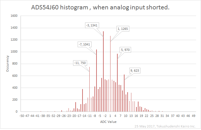
ADS54J60: Bad histogram and DNL. One comb in four.

Part Number: ADS54J60
Other Parts Discussed in Thread: ADS54J40, , LMH6401, TSW54J60EVM

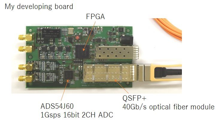
I am developing an 1Gsps ADC board using ADS54J60.
It sends data by JESD204B using optical fiber.
The operation of JESD204B is going well.

Taking a code histogram at the input voltage difference is 0, it was like a comb !
When the least significant bit of the ADC code is "01", it seems to be larger.

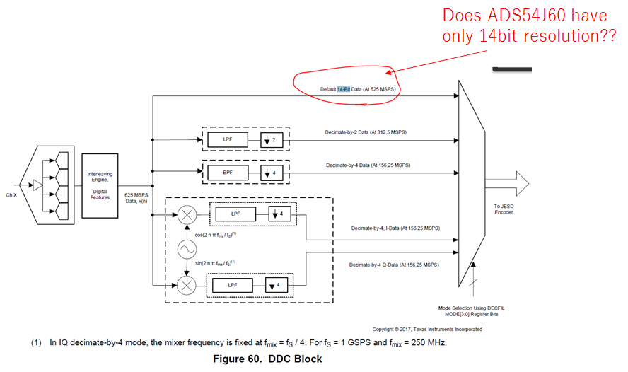
According to the datasheet there is a description "Default 14-Bit Data" on Fig.60.
Does ADS54J60 have only 14bit resolution??

Condition is following.

LMFS config is 4211.
K=16
N=5
SYSREF=1.953125MHz ( = 1GHz / 32 / 16)

Please tell me the reason for this.

Best regards,
Ryuji Naitou

  • Ryuji,

    That is a typo on Figure 60 of the data sheet. It is suppose to be 16 bit. Do to the operation of the DC offset engine, the data converter output will try to be correct for a DC level signal, which is why you are seeing these results. Try this test by disabling the DC offset correction, per the attached document. 

    Regards,

    Jim

    ADS54J60_DC_CORR_External.pdf

  • Hi Jim.

    I understood that one ADC of ADS54J60 consists of four ADC cores and working of DC corrector.
    And I also tested external offset and confirmed that it works properly.

    If the DC correct ion mechanism does not work well, indeed, I confirmed waveform in time domain will be a comb one of four.
    But what I am in trouble is that not waveform but the code density histogram is a comb .

    The mechanism of DC correction gave me a great hint.

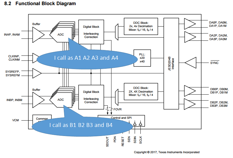
    ADC A and B are each consist of four 250 MHz ADCs in ADS54J60.
    I call them ADC A1, A2, A3, A4, B1, B2, B3 and B4 here.

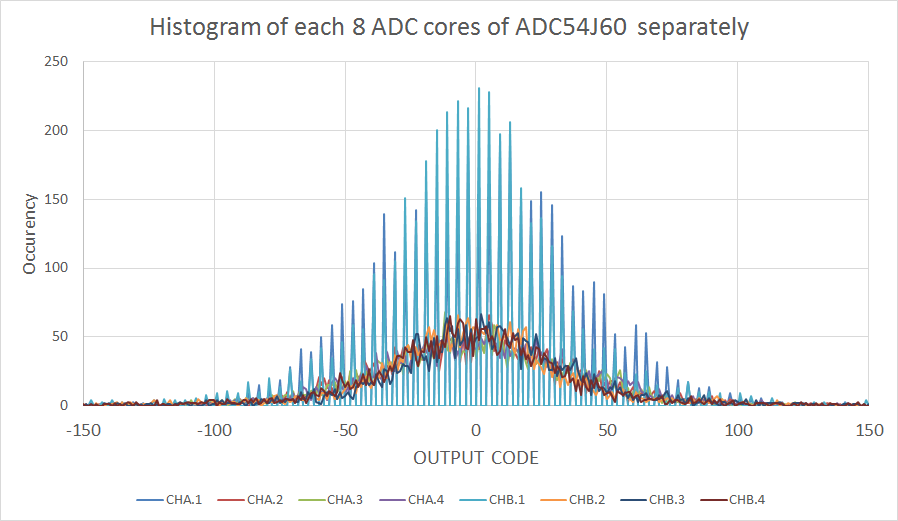
    I tried to make histograms separately for the codes output by these eight ADCs.

    I attach the figure.

    I divided this into A1, B1 and others.

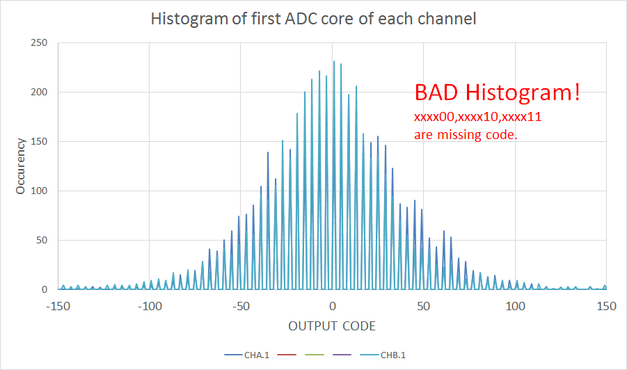
    Please see histograms of first 2 cores.

    ADC A1 and B1 are outputting only the code whose LSBs are "01" !
    Every "00", "10" and "11" are missing codes !!

    It seems that ADC A1 and B1 have only 14 bits of precision.

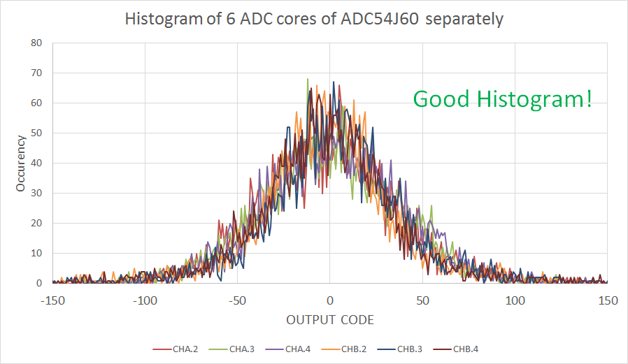
    Other ADCs, i.e., A2, A3, A4, B2, B3, B4 are outputting good histograms and they have 16 bit resolution.

    Why are the resolutions of two of the eight ADC cores low?

  • Ryuji,

    Do you have a TSW14J56EVM to capture the data with? If so, can you capture the data and place the display in bits mode to verify all 16 bits are toggling. We have had a case were some EVM's had 16 bit parts fused as 14 bit parts instead by accident.

    Regards,

    Jim

  • Hi Jim.

    Thank you for reply.
    No, I don't have an EVM.

    I use my handmaid board. (photo above)
    Least significant 2 bits (of only one lane per ADC) are not toggled in normal operation.
    But all 16 bits are toggled when JESD204B scramble enabled, so my data decode logic and ADC's digital block seems good.

    My ADC's silk is "Z54J60 TI 594 ZRFK G4".
    I bought this on Oct 2016?as an IC part.
    Is this also an accident product?

    Regards,
  • Ryuji,

    You mention 2 LSB's are not toggled in normal operation. To me it appears you have a 14 bit part (ADS54J40) on your board. Have you tried replacing the device? If not, I would suggest you do. How many of these parts did you order? I can send you replacement parts if needed.

    Regards,

    Jim 

  • Hi Jim.

    I bought total 3 parts at Digikey. Remaining 2 parts are not implemented yet.

    >To me it appears you have a 14 bit part (ADS54J40) on your board.

    I bought ADS54J60 surely and the silk is "AZ54J60".

    There is another thing to worry about.

    In the ILAS, the N =14. Is this correct?

  • Ryuji,

    No. N should be 16. I think your part was accidently built as a 14 bit part but labeled as a 16 bit part. I have come across this in the past.

    Regards,

    Jim  

  • Dear Mr. Jim.

    I bought two ADS54J60 at Digikey and one at TI's online store.

    The silk description is same.

    "AZ54J60 TI 594 ZRFK G4" on three ADS54J60.


    I replaced one of them and tried again with the new part.

    However, the result did not change. The histogram was "comb-like" with 1 in 4.

    Also, looking at the ILAS frame also shows N = 14. Even though it is ADS54J60.

    Why does the N become 14 ?

    The silk of the four parts was the same and it seems that parts of TI's online store came out from the warehouse of Digikey (Digikey-like invoice and from same address)

    So it may not change the result even if changing parts anymore.

    Is there a possibility that it will be 14 bits due to user's wrong SPI operation ?

  • Ryuji,

    we would like to verify if there is possibly anything wrong with the devices you are using. Our customer support will contact you for replacement of your devices and return of the ones you have right now.

    Matthias
  • Ryuji,

    Does you board provide the required power sequencing needed by the ADS54J60 per the data sheet? We noticed on one of our EVM's where we did not do this, one of the channels was configured for 14 bit instead of 16 bit. After applying the correct power sequence, this problem went away.

    Regards,

    Jim

  • Dear Jim,

    I have a same issue on the ADS54J60EVM.

    ADC resolution is only 14bit after revised power sequence.

    I'd like to confirm you mentioned "power sequence".

    It means that the 1.15-V IOVDD supply must rise before the 1.9-V DVDD supply.

    Is it correct?

    Regards,

    Kei  

  • Kei,

    That is correct. Can you go to page 0x6100 and read address 0x0F and let me know what the value is?

    0x4004 0x61

    0x4003 0x60

    Read address: 0x600F

    Regards,

    Jim

  • Hi Jim,

    Thanks for your prompt reply.

    I read 0x6100 0x0F by ADS54Jxx GUI, but the value is always 0.

    0x600F is same as well.

    Is it possible to read hidden pages and resisters by this GUI?

    I measured the power sequence on ADS54J60EVM without any modification.

    Attached please confirm it. Is this a reasonable?

    Regards,

    Kei

  • Hi Jim and kei.

    Our situation is exactly the same.

    The 600F hidden register is 0.
    I heard that means 16bit mode.

    Since our board is made referring EVM, the circumstances of power supply are the same.
    DRVDD will rise later but since IOVDD is leaking to DRVDD, they will rise together until 1.15V.

    We are asking for support vir TI Japan but it is not yet solved.
    It is said that synchronization of SYNC to CLK is suspicious.
  • Ryuji,

    As a test, can you disable DRVDD and make sure you do not turn it on until IOVDD is at 1.15V?

    Regards,

    Jim

  • Kei,

    You can read any register with the GUI as long as you set the page correctly first. I am assuming you did the first two writes first at 4004 and 4003 before the read of address 600F, correct? I do not like the view of the power sequence. Make sure IOVDD is at 1.15V before turning on DRVDD.

    Regards,

    Jim

  • Ryuji,

    If you are using the ADS54J60EVM, can you replace C184, which is near U8, with a 1uF cap? This should delay the start up time of DRVDD1.9V.

    Regards,

    Jim

  • Ryuji,

    Can you try the following on your setup:


    1. It appears ADC Bit 1 is stuck. Need to do the writes below.

      By default OVR is sent on Bit 1. This register puts the ADC output on bit1.


    0x4004 0x6A

    0x4003 0x00

    0x6012 0x02 // Always write 1 bit added in latest datasheet.


    Regards,


    Jim


  • Hi Jim.

    When I set this register, ths behavior has surely changed but it is not perfect.
    I will report detail tomorrow.
  • Hi Jim.

    I tried add following register setting and measure histogram 5 times.

    0x4004 0x6A -- hidden page

    0x4003 0x00 -- hidden page

    0x6012 0x02 -- Always write 1 bit added in latest datasheet.

    0x4004 0x68

    0x4003 0x00

    0x6052 0x01 -- Set gain validity

    0x6044 0x21 -- set default gain to +0.25dB

    0x60AD 0x04 -- Always write 0x04 ( datasheet is updated)

    0x60AB 0x01 -- validity for LSBbit select

    0x6000 0x01 -- digital core reset

    0x6000 0x00 -- digital core reset remove

    As a results, histgram was changed obviously.

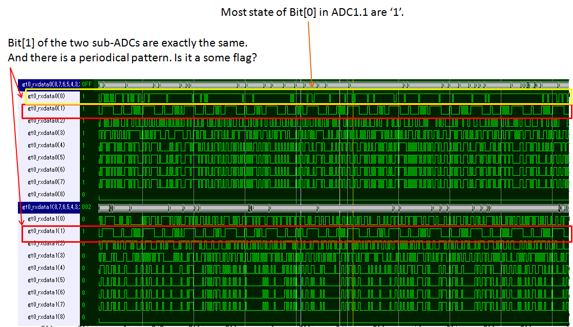
    From the least significant 2 bit, ADC data and fixed value are output alternately with the passage of time.

    And by this modifing, bit[0] is seemed ADC data but I thought  bit[1] is not ADC data.

    Each bit[1] of four sub ADCs are  same value and periodically change

    It seems the resolution is 14 bits practically.

  • See my private post.
  • Hi Jim

    Where is your post?

    Thank you
  • Ryuji,

    I sent you a friend request. Did you get it?

    Regards,

    Jim
  • Hi Jim
    I got a friend request and accepted it.
    I can see you in my friends list.
  • Did you get my latest post then? Please reply as a friend.
    Jim
  • Hello all,

    Do we have any resolution on the comb histogram issue? I have the same issue on my board. More than that: doing decimation by 4 (reading just one sub converter), the comb histogram change randomly with the normal smiling face after resetting the ADC.

    Nestor
  • Nestor,

    Try the following writes in the attached document.

    add these writes before you do the digital core reset:

    Address, Data
    0x4004 0x68
    0x4003 0x00
    0x6052 0x01 // Set gain validity
    0x6044 0x1F // set default gain to -0.25dB
    0x6000 0x01 // digital core reset
    0x6000 0x00 // digital core reset remove


    Regards,

    Jim
  • Hi Jim,

    Thanks for the answer. I am doing that already. The default value doesn't remove the clipping waves but higher gain will do it.
    The question is: does this lower the ENOB. If the digital gain is a simple multiplication, the ENOB will be affected. If it is more complex than that, it may work without affecting the ENOB.

    Nestor
  • Nestor,
    I am checking with the design team regarding this.
    Jim
  • Thanks Jim.
    By the way, do you have any news on the comb histogram?

    This is the code I am using to set the ADC:

    void ADC_Init(int adc)//0,1 accepted
    {
    int dev = (adc==0)?0:1;
    int data = 0; int reg = 0;

    //Reset the device
    data = 0x81; reg = 0;
    WriteToADCReg(dev,reg,data);

    //Enable broadcast
    data = 0x0; reg = 0x05;
    WriteToADCReg(dev,reg,data);

    //Clear unwanted content
    data = 0; reg = 0x4001;
    WriteToADCReg(dev,reg,data);
    reg = 0x4002;
    WriteToADCReg(dev,reg,data);

    //**********************************//
    //Select Main dig page JESD(0x68)
    //**********************************//
    data = 0; reg = 0x4003;
    WriteToADCReg(dev,reg,data);
    data = 0x68; reg = 0x4004;
    WriteToADCReg(dev,reg,data);

    //Dig Reset self cleaning
    data = 1; reg = 0x60f7;
    WriteToADCReg(dev,reg,data);

    //Set Nyquist
    data = 0; reg = 0x6042; //default: 0..500Mhz
    WriteToADCReg(dev,reg,data);

    data = 0x80; reg = 0x604E; //Nyquist EN
    WriteToADCReg(dev,reg,data);

    //Set Digital Gain
    data = 0x21; reg = 0x6044; //default: 0x20 (0x21 is the min to remove the clipping wave)
    WriteToADCReg(dev,reg,data);

    data = 0x01; reg = 0x6052; //Digital Gain EN (default 0)
    WriteToADCReg(dev,reg,data);


    //Pulse the reset
    data = 1; reg = 0x6000;
    WriteToADCReg(dev,reg,data);
    data = 0;
    WriteToADCReg(dev,reg,data);

    //**********************************//
    //Performance mode
    //Select the master page of analog bank(0x80)
    //**********************************//
    data = 0x80; reg = 0x0011;
    WriteToADCReg(dev,reg,data);

    //EN INPUT DC COUPLING
    data = 0x01; reg = 0x004F;
    WriteToADCReg(dev,reg,data);

    //Always write 1 bit
    data = 0x20; reg = 0x0059;
    WriteToADCReg(dev,reg,data);
    //Performance mode END

    //**********************************//
    //Program the JESD registers
    //Select the JESD dig page (0x69)
    //**********************************//
    data = 0; reg = 0x4003;
    WriteToADCReg(dev,reg,data);
    data = 0x69; reg = 0x4004;
    WriteToADCReg(dev,reg,data);

    //Set the CTRL K bit for chA+B
    data = 0x80; reg = 0x6000;
    WriteToADCReg(dev,reg,data);

    //Set LINK LAYER TESTMODE
    data = 0x00; reg = 0x6002;
    WriteToADCReg(dev,reg,data);

    //JESD MODE LMFS=4244 (0x02)
    data = 0x02; reg = 0x6001;
    WriteToADCReg(dev,reg,data);

    //Set SCRAMBLE DISABLE (0x05)
    data = 0x00; reg = 0x6005;
    WriteToADCReg(dev,reg,data);

    //Set the value of K and SYSREF (0x1f)
    data = 0x1f; reg = 0x6006; //choose K value = 32 as on initial core setup
    WriteToADCReg(dev,reg,data);

    //Set JESD204 subclass 1 (0x08)
    data = 0x08; reg = 0x6007;
    WriteToADCReg(dev,reg,data);

    //**********************************//
    //Select JESD analog page (6A)
    //**********************************//
    data = 0; reg = 0x4003;
    WriteToADCReg(dev,reg,data);
    data = 0x6A; reg = 0x4004;
    WriteToADCReg(dev,reg,data);

    //Set JESD PLL MODE: 40X mode, two lanes per ADC (0x02)
    data = 0x02; reg = 0x6016;
    WriteToADCReg(dev,reg,data);

    //It appears Bit 1 is stuck since the default setting of this device is send OVR to bit 1.
    //Please do these writes below to assign the ADC output to this bit.
    //These writes will be added to the data sheet in the next revision.
    data = 0x02; reg = 0x6012;// Always write 1 bit added in latest data sheet.
    WriteToADCReg(dev,reg,data);

    //PLL Reset
    data = 0x40; reg = 0x6017;
    WriteToADCReg(dev,reg,data);
    data = 0x00;
    WriteToADCReg(dev,reg,data);

    return;
    }
  • Nestor,

    Regarding your question about digital gain:

    The digital gain programmed is only 0.25dB in this example we sent you.

    If you have 70dB SNR, ENOB = (70-1.76)/6 = 11.33bit

    With gain of 0.25 this is 70-0.25 = 69.25dB SNR, ENOB = (69.25-1.76)/6 = 11.24bit


    With this gain feature, you can also provide attenuation in the digital block, which will improve the SNR.

    Regards,

    Jim

  • Thanks Jim. Yes indeed this make sense.

    Unfortunately right now we have a ENOB around 10 bits and this is related to the "comb histogram".

    I am eager to know if there is a solution for that.

    Regards

  • Nestor,

    What sample rate is the ADC? Is this on board CLK or external? If external, is the clock filtered? What is the IF? Is this filtered? What mode is the ADC using?

    Jim

  • Jim,

    The ADC is ADS54J60 running at 1Gs/s (two of them) and the clock is provided by the LMK48028 on the board. Like frontend we use LMH6401 and is DC coupling.

    We use a 500Mhz filter on board.

    The JESD204 IF is LMFS=4244, K=32. Working with Patrice P. on the same project.

    Regards

  • Is this a TI ADS54J60EVM modified to bypass the input transformers? We have another board called the TSW54J60EVM that has a LMH6401 connected to ADS54J60. Attached is some info regarding this board and the interface between the two parts. See if this helps you.

    Regards,

    Jim

    tidub15.pdf

  • Jim,

    Thanks for the link. Me, I didn't see this file before but we build our own board similar to that.

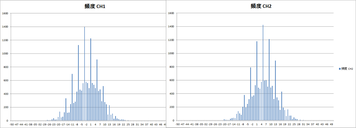
    We invest a lot of time to understand what happens with the histogram of the single converter (ADC channel samples decimated by 4) and why are missing, some time, 3 out of 4 consecutives values.

    I have attached a few screen grabs with good or bad histograms. I am running a command between captures (see the code below) that randomly change the look of the histogram.

    //Command used for DC level calibration

    int DC_freeze (int option)
    {

     //select page 0x61000000, adc0
     WriteToADCReg(0,0x4004, 0x61);
     WriteToADCReg(0,0x4003, 0);
     WriteToADCReg(0,0x4002, 0);
     WriteToADCReg(0,0x4001, 0);

     //unfreeze DC adc0
     WriteToADCReg(0,0x6068, 0x02);
     // Disable external offset correction
     WriteToADCReg(0,0x6069, 0);

     //select page 0x61000000, adc1
     WriteToADCReg(1,0x4004, 0x61);
     WriteToADCReg(1,0x4003, 0);
     WriteToADCReg(1,0x4002, 0);
     WriteToADCReg(1,0x4001, 0);

     //unfreeze DC adc1
     WriteToADCReg(1,0x6068, 0x02);
     // Disable external offset correction
     WriteToADCReg(1,0x6069, 0);

     //Do DC 0 V adjust ch 1+2: adjust the offset dacs for ~0V reading
         if (DC_ZeroV(0,option) < 0) return (-1);


     //freeze DC adc0
     WriteToADCReg(0,0x6068, 0x82);

     //Do DC 0 V adjust ch 3+4: adjust the offset dacs for ~0V reading
         if (DC_ZeroV(1,option) < 0) return (-1);

     //freeze DC adc1
     WriteToADCReg(1,0x6068, 0x82);


    return 0;

    }

    Bad Histogram


    Good histogram


    Bad Histogram Zoom in


    Normal Histogram zoom in


    Help me to understand what's happening.


  • Nestor,

    Can you please tell us what application this is to be used with and why is this such an issue? This was requested by the design team and may allow them to provide you with an answer. Are you getting this bad histograms with the new register settings we sent you? Do these occur after every power cycle? Are you working with Kyuji on the same project?

    Regards,

    Jim
  • Jim,

    This a 4 channels acquisition board and we are expecting to have a ~11bits ENOB.

    You ask if I am getting this histograms with the new registers settings: registers 0x6052/0x6044 settings helps for the "clipping wave" issue but not for the histogram.

    Do these occur after every power cycle?: Yes

    I am working with Patrice Plante. I do not know Kyuiji.

    Regards

  • Jim,

    I want to be more precise on the digital gain registers: digital gain enabled with a value >=0x21 will remove the "clipping wave" but the histogram will be always "bad".

    With the digital gain disabled or enabled but =< 0x1F the histogram will switch randomly from "bad" to "normal" after each "DC level calibration command" (DC_freeze).

    Regards

  • Jim,

    Do you have any news on the histogram issue?

    Regards