This thread has been locked.

If you have a related question, please click the "Ask a related question" button in the top right corner. The newly created question will be automatically linked to this question.

TLV5616 DAC - SPI: Sending Data Twice?

Other Parts Discussed in Thread: TLV5616

Hello,

I'm using a TLV5616 12-bit DAC, and controlling it via SPI from an Atmel 8-bit AVR processor (AT90USB1286) (A Teensy 2.0++):


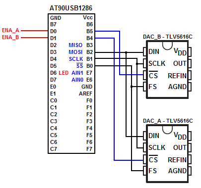
I'm controlling the /CS and FS lines from software. Only SCLK and MOSI are controlled automatically via the chip's SPI module.  Currently, it is working, and I am seeing the expected DAC output, however, in order to change it, I need to send the data twice. Any ideas why?

First, I'm not positive as to which SCLK settings to use.  There are two options: one for SCLK Polarity, and SCLK Phase. Since the TLV5616 datasheet says data are clocked in on the falling edge of SCLK, I have my SCLK polarity set to inverted (CPOL=1).  Phase is normal (CPHA=0).  Does this sound correct?  The Atmel datasheet refers to these 4 combinations as Mode 0, Mode 1, etc. and I have it configured in Mode 1.  In other words, which SPI mode does this DAC expect SPI data?

Second, (this may be related), does anyone have any idea why I would have to send my data twice to the DAC, in order to get it to update? I have an LED blink to verify the data is being sent, and I see my CS and FS lines go low.  The datasheet says the DAC should update After the 16th bit is sent, or FS goes high.  Here is my code (just testing one DAC, although two are part of the design).

PORTB &= ~(1<<PB4);  	// /CS on DACA low
PORTB &= ~(1<<PB0);
// FS Low
// Send Data MSB (bit and byte) First. 
SPI_MasterSend( (SPD_CTRL<<6) | (val_high & 0x0F) );	// Byte 0
SPI_MasterSend( val_low );				// Byte 1
PORTB |= (1<<PB0);		// FS High
PORTB |= (1<<PB4)|(1<<PB5); 	 // Both /CS High

I've tried just about everything, to no avail: Adding delays between all signal line transitions, Slower SCLK, All combinations of CPOL and CPHA, and even eliminated /CS, by tying it to ground.  Any suggestions?


Thank you very much,

Jonathon Reinhart

  • Hi Jonathon,

    For the SPI interface, both (1) CPOL = 0, CPHA = 1 and (2) CPOL = 1, CPHA = 0 should work, as both of those modes will set the SPI to sample on the falling edge of SCLK. Option (1) is useful if you want the DAC output to update with the FS rising edge, since the clock dwells low and there will not be a rising SCLK edge after the 16th falling clock edge in a 16-bit write. When using (2), the DAC output will update when the clock returns high after the 16th falling SCLK edge to sample the LSB.

    Just to clarify, after power up, you need to send the 16-bit write twice for every DAC output update? Or is it only after the initial write after powerup, i.e. after the first write that does not update the DAC output, every consequent write command updates the output correctly?

    Give this a shot:

    1. Use CPOL = 1, CPHA = 0
    2. Tie /CS low
    3. Dwell FS low during/after the TLV5616 power up
    4. For a write command, pull /FS high then low (making sure the minimum 20ns FS pulse width requirement is met) and then send in the 16-bit command/data. The DAC output should update when SCLK returns high

    Please let me know how it goes.

  • Hi Kristoffer,

    Thanks for the quick reply.  I discovered my problem; such a stupid mistake:

    (1<<CPOL)     // Correct
    (CPOL<<1)     // WRONG!

    Thank you for your help, and also explaining the SCLK options.  I'm doing what you described: FS low at idle, and just sending a short pulse before write command. CPOL = 1, CPHA = 0, and 16th bit initializes the transfer to DAC latch.

    Best Regards,

    Jonathon Reinhart