This thread has been locked.

If you have a related question, please click the "Ask a related question" button in the top right corner. The newly created question will be automatically linked to this question.

DLP9000 / DLPC900: Left half image with artifact

Part Number: DLP9000XUV
Other Parts Discussed in Thread: DLP9000, TPS65145, DLPC910, DLPC900, , DLPLCRC900DEVM

Dear forum members,

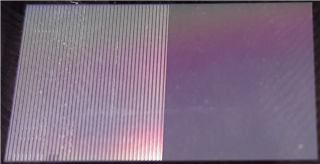
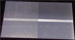
We're having the following issue with our DLP9000 DMD, first half of the image always shows artifacts, it looks like vertical stripes, however it's not homogeneous. In the attached pictures, one image should show only black background, and the other one should show a horizontal white band with black background.
Context:

- Board needs to be reset some times before it can stand in normal mode and allows an operation mode to be selected.

- Even when pattern on the fly mode gets seleceted and sequence gets updated and started, not always can be visualized. This correlates with the voltages generated by the TPS65145 for the DMD in the following way: most of the times TPS65145 shutdowns as soon as it powers on even with enable input high (overload detected?), and sequence is not visualized. When TP65145 can make it to stay on and generates the proper voltages (16V, 8.5V, -10V) then the sequence is visualized.

- Master controller gets noticeable hotter than the slave controller (maybe it's related with the half of the image showing the artifacts), I would say it's definitelly overheating.

- The four main regulators on the controller board were already checked (1.8V, 1.1V, 3.3V and 3V).

- The cLGA socket between DMD and PCB was replaced for a new one.

We really appreciate your help.

Marcos.

  • Marcos,

    I need to ask a few questions before proceeding so that my answers are addressing the system you have.

    Are you using the DLPC910 as the controller?  Because you mention two controllers - primary (formerly master) and secondary (formerly slave).

    The DLP9000(& XUV) are intended to be driven with the DLPC910, or are you using two DLPC900's?

    I counted the stripes and there are 40 pairs of the stripes in the left half.  If I do the math [ (2560/2)/(2*40) = 16 ] shows that each strip is 16 pixels wide.  I also notice a lot of pixel noise even in the right half of the white stripe.

    This would point a noisy input on one of the two busses of the two primary side inputs and some possible noise on the other side also.

    The places to looks would be:

    • Clock inputs on the primary side (and similar for the pixel noise on the secondary side.
      • Particularly check to see if one bus is significantly worse. The 16 pixel wide strips point to one bus being noisy.
      • These can be due to poor Ohmic contact at the solder points, vias, flex cable.
    • Check the SCTRL lines.  This is less likely as a malformed packet would likely result in no data being shown.
    • Please also check the flex cable interfaces to see that there is no trash/debris or residue on the contact pads or on the "pins" at both ends.
    • Check data lines, but this is very unlikely since it would show up as single pixel wide vertical stripes every 32 pixels.

    Fizix

  • Hi Fizix, thanks for your quick response,

    System is using a dual DLPC900 controller board (DLPC900D?) with a master and slave controller chips (both DLPC900). Actually it's recognized as DLP9000 in the GUI, however it's the only radio button available there for the DLP9000 series. 

    Regarding data cables, we have reviewed, cleaned the contacts and reseated them like 3 times, we have also cleaned the DMD chip and PCB contacts, and have replaced the interposer for a new one (also reseated once).

    Some context:

    This DMD system is part of a 3D printing device, and resin leakage was found all over the DMD board, interposer, cable contacts and over controller board, specially at the corner where the voltage regulators are located. In fact 1.8V power supply was damaged and repaired. All is clean now.

    We have performed 2 additional tests:

    • unmounted DMD chip and manually enabled the TPS65145: it properly turned on every time, all voltages ok, no shutdown
    • disconnected data cables from controller board: master controller chip quickly rises its temperature, can this suggest a short circuit in the chip?

    You are right regarding the observed noise on the right half side, would that mean a damage common to both halves? noisy power supply?

    We'll be performing the measurements you have indicated, clock inputs are the clocks of the LVDS buses to the DMD right? do you know the required bandwith for measuring?

    If I understood correctly, there are 2 LVDS buses per side, i.e. 2 differential clocks per side, and one is expected to be worse, right?

    We'll be giving you feedback as soon as we have the measurement results.

    Thanks a lot,

    Marcos.

  • Hi Marcos,

    Thank you for the additional details. Yes, there are two buses per side. You can review section 9.2 of the DLP9000 datasheet on ti.com for the very high level block diagram.

    You mentioned that the resin got onto the boards and components. Was the system working fine before the resin event?

    Regards,

    Matt

  • Hi Matt, thanks for your response,

    We believe this leakage occurred over time, and system may have gone through a gradual performance degradation. There was a serious leakage incident some months ago, however system did not fail immediately after. We can tell for sure that when we opened the case there was resin and dirt all over the controller board, with some corrosion on the corner where the four main regulators are located (1V8 supply had to be repaired). Also we've found resin under DMD chip, the interposer was fully embedded with resin, actually we had to replace it as many c-springs were broken. There was also leakage in the cable contacts.

    I'll answer Fizix separately.

    Please ask anything you need or suggest any measurement you'd like to perform.

    Regards,

    Marcos.

  • Hi Fizix, thanks for your support.

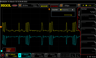
    Regarding your suggested measurements, we have performed LVDS diff. clocks and control signal measurements right on the vias under controller ICs, using the ground spring for the scope probes. We have used a scope with insufficient bandwidth, however fundamental frequency and complimentary phase can be identified, tomorrow we'll be repeating the measurements with a higher bandwith scope.


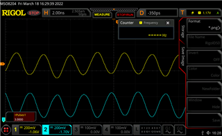
    This is a capture of the DCKB_P and DCKB_N LVDS diff. clock for slave controller; similar waveforms were obtained for the other 3 buses:


    These are captures of the SCx_P and SCx_N diff. control signals for the 4 buses:

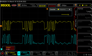
    Slave bus SCB (slave controller pins J1 and J2, nets S_SCTLA_x):


    Slave bus SCA (slave controller pins V1 and V2, nets S_SCTLB_x):


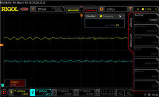
    Master bus SCB (master controller pins J1 and J2, nets M_SCTLA_x), apparently no signal and it correlates with affected image half:


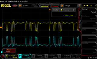
    Master bus SCA (master controller pins V1 and V2, nets M_SCTLB_x):


    Even though scope bandwith is limited, apparently control signal for one of the master buses is missing, which seems to correlate with the image half showing the stripes.

    Tomorrow we'll repeat the measurments with a 2GHz BW scope.

    Please ask anything you need or suggest any measurement you'd like to perform.

    Best regards

    Marcos.

  • Hi Marcos,

    Thank you for the explanation of the resin issue.

    Based on your measurements, yes, one bus is having a problem after the boards have been cleaned up. Fizix can review and provide feedback on next steps.

    I do want to clarify one of your earlier comments: the dual DLPC900 controller board is what you are using, and the DMD EVM has the DLP9000XUV DMD on it. Is this correct?

    Currently, the DLPLCRC900DEVM user guide (DLPU102) does not list the DLP9000XUV DMD as a supported device. The DLPC910 controller is the device to pair with this UV DMD. My concern is that there might be an issue connecting with this DMD, or in operation. 

    We will need to review this more closely.

    Regards,

    Matt

  • Sorry Matt, my mistake, exact P/N for DLP is DLP9000FLQ.

    Thanks,

    Marcos.

  • Thank you Marcos. Glad to see there should be no chipset connections issues. I will check with Fizix to see what other info we can provide today.

    Matt

  • Marcos,

    I am surprised that you are getting anything at all on the side that has a missing SCTL signal(s).  The pairs form one packet of information.  If we label one side of the DMD as bus A & B and the other side as C & D, the SCTLA+SCTLB form one packet and their information is not identical.  Similarly for C & D.  C+D is a copy of A+B.

    Let us know the result of looking at this with the higher bandwidth scope.  This appears to be pointing in the right direction.

  • Thank you Matt!

    Regards,

    Marcos.

  • Hi Fizix,

    Here are the captures with the other scope, however these look very similar.

    LVDS clocks still look sinusoidal (the same for all buses):

    Control signals SCx:

    Master SCA_P and SCA_N:

    Master SCB_P and SCB_N (We have measured resistance from each line to ground to rule out a short circuit; values are similar to the other buses):

    Slave SCA_P and SCA_N:

    Slave SCB_P and SCB_N:

    Have a nice weekend.

    Regards,

    Marcos.

  • Marcos,

    Clearly there is a bad connection on the Secondary (formerly slave) Controller SCTL A line.  That must be traced down and fixed before any other significant debug can be performed. 

    I am a little concerned that the clocks look so sinusoidal.  I expect them to be somewhat rounded out, but not quite that much.  Do you know what impedance the inputs are set at?  I would expect 1 MOhm or better.  Also, how long are the leads?  Ideally a differential probe would improve the signal a bit.  I expect they are likely ok.

    Let us know how your investigation proceeds.

    Fizix

  • Hi Fizix,

    Regarding the clocks shape, I was also expecting more like a damped pulse, however regarding scope and probe specs, we've used a Rigol MSO8204 2GHz BW, 10Gsps scope, with RP3500A 500MHz, 10Mohm, 10:1 probe, with probe autoconfig, and full BW selected.

    Regarding missing control signal (Master SCB_P and SCB_N), we've actually measured directly on the J1 and J2 pin vias, on the other side of the controller IC, do you mean a bad solder joint of the pad to the PCB?

    Regards,

    Marcos.

  • Hello Marcos,

    I was mentioning the places to look.  From where you measured it sounds like it would likely be upstream, maybe at the IC to pad solder joint.

  • Fizix,

    Without the DMD connected we still measure high state in both SCB_P and SCB_N vias under the master controller IC, so there is electrical contact between IC and PCB pads, unfortunately there's no signal generated from the controller, a bad sign.

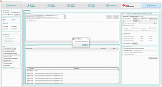
    As a last try, we're trying to reflash the firmware, however we're getting an unknown flash IDs error:

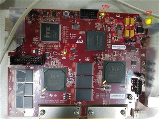
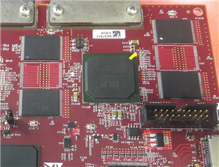
    At first we thought it was related to a misconfiguration in the FlashDeviceParameters.txt, however the installed device M29DW128G is correctly specififed, we think it may be related to the number of installed ICs, while in DLP9000 kit all the 6 positions are populated, in our board only 4 ICs are installed:

    DLP9000 kit:

    Our system:

    Regards,

    Marcos.

  • Marcos,

    I am sending you a friend invitation on this.

    Fizix

  • Marcos,

    Through our private discussions I believe we figured out that the Chip Select for the second  of the two flash chips per controller was incorrect.  The data sheet shows CS1, CS2, and CS0 in that order, but your board was CS1, then CS0 but the controller is expecting CS1, then CS2 for only two chips.

    I am marking this resolved and closing the ticket.  If you need further help please open a new ticket.

    Fizix

  • Hi Fizix, I hope you're fine these days,

    Regarding the "dead" control bus in master controller, i.e., both lines at high state, at that time you have concluded that probably both lines are shorted and one is pulling high the other, however I forgot to mention that I had already measured resistance of both lines to ground and got a high value, similar to the other buses. Hence we have discarded a short between N and P lines, and concluded that it may be an issue internal to the controller (also it overheats). Currently we're not going forward with the fix, but are waiting for new stock of a DLP900 dual EVM board to be available to purchase one.

    Once again, thanks for your time and your excellent support.