Other Parts Discussed in Thread: DLP300S, DLP301S
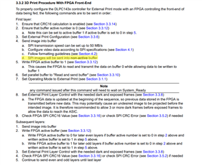
In section 3.3.2 3D Print Procedure With FPGA Front-End (Page 33) step 4, the guide states that SPI images are sent into non-active buffer
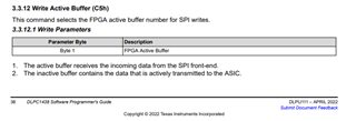
But, in section 3.3.12 Write Active Buffer (pg 38), it states the following:
1. The active buffer receives the incoming data from the SPI font-end.
2. The inactive buffer contains the data that is actively transmitted to the ASIC.
To me, unless I'm misunderstanding, I'm assuming a system with an FPGA buffer works as follows:
1. Set active buffer to buffer 0.
2. Send an image into buffer 0.
3. Change buffer 1 to active and buffer 0 to inactive. This sends the data from buffer 0 through the parallel lines, to the controller, and then into the memory cells of each micromirror.
4. When commanded to expose n frames via the external print layer control command, the controller sends a global clocking pulse to the DMD to update all mirror positions.