This thread has been locked.

If you have a related question, please click the "Ask a related question" button in the top right corner. The newly created question will be automatically linked to this question.

DLPC231-Q1: What's the skew margin mean for DLPC231

Part Number: DLPC231-Q1

Hi TI expert

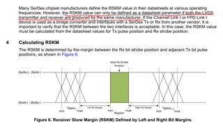
According the snla249 mentioned , there are three part of skew parameter defined .

1.Transmitter pulse variation.

2.RSKM

3.Receiver Strobe Window.
Can you help to clarify in DS of DLPC231-Q1, tskew listed below represent to RSKM or strobe window?

BR Jingcheng

  • Which transmitter part number are you using or considering?  We need to find an expert on the FPDlink team that can help address this question and the others that you have.  The openLDI on the DLPC230/DLPC231 is a hard coded phy which is compatible to the standard, but we do not have detailed expertise on this team on the protocols.  Therefore, I want to move this question to the right team.

  • Hi Jason

    DLPC230-Q0 is using.Please help move this question to the right team.

    BR Jingcheng

  • JingCheng,

    The Tskew is the same as RSKM from the app note.  In this case of the DLPC230 the max amount of skew for any bit must be equal or less than 400ps.

    See section 6.14 of the datasheet.

    Jason

    https://www.ti.com/lit/ds/symlink/dlpc230s-q1.pdf 

  • Hi Jason

    The RSKM is determinated by UI/Rspos/Tppos parameter, normally the RSKM will not be provided in Datasheet,as TX IC type is unknown. 

    Do the 400ps RSKM defined precondition is TX IC has detailcate type defined ?

    0.5UI = 0.5Tppos + RSKM + 0.5Rspos 

    BR Jingcheng

  • HI Jason

    If the Tskew is same with RSKM .according the SNLA249 defined, i thinke the Max amount of skew for any bit must be equal or less than (400ps + 0.5Tppos + 0.5Rspos) ,but not 400ps .

    BR Jingcheng

  • JingCheng,  you may be right.  We are not experts on the details of the SNLA149 document.  However, in discussing with the HW designers, the T_skew must be the final amount of skew between clock and data at the input of the DLPC230.  Also, T_jitter will reduce the margin further.  The app note should be used to calculate all factors that would reduce the margin.  The DLPC230 receives the clock and data and it must not exceed 400ps of margin at its input @ 85Mhz.  Also, T_jitter would reduce this margin further.  Let me know if this clarifies what is required for the DLPC230.

  • Hi Jason

    Thanks for your update.

    "However, in discussing with the HW designers, the T_skew must be the final amount of skew between clock and data at the input of the DLPC230."

    Can i used the 400ps substract driver side Tx_total_Skew and get skew margin for Interconnection part(PCB trace  + connector + crosstalk ect.)?

    For example , i used the Tx_total_skew = +/-180ps@85Mhz LVDS driver IC, and receiver is DLPC230, the skew margin for interconnection part should be 400- 180 = 220 ps. Is my caculation correct?

    BR Jingcheng

  • JingCheng,

    Yes this is correct.  Then, if you also had another 100ps of cycle to cycle jitter, then the total margin would be reduced further to 120ps.  In this case, everything should add up and work properly.

    Jason