This thread has been locked.

If you have a related question, please click the "Ask a related question" button in the top right corner. The newly created question will be automatically linked to this question.

DLP4710LC: DLP4710EVM-LC

Part Number: DLP4710LC
Other Parts Discussed in Thread: DLP4710EVM-LC, DLPC3479, DLP4710, DLPA3005, DLPC900,

Tool/software:

Dear 

I am reviewing DLP4710EVM-LC reference schematic and data sheet to develop 3d scanner.

I’m sorry for asking so many questions.

[Q0] In the reference schematic, it seems that only the Trigger0/1 of the Master beam is available. When capturing in Camera Trigger Mode, is it sufficient to use only the Master DLPC3479?

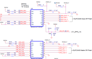
[Q1] The USB SPI is connected to both the Master SPI and Slave SPI through resistors.

        In this configuration, it seems like there might be a conflict with the SPI signals from the DLPC3479. Is it possible to proceed with downloading data in this setup? Could you explain theoretically?

[Q2]To use the same circuit as the TI EVM for downloading, are there any considerations we need to take into account when controlling the DLPC3479 or when developing our own download program?

[Q3] When using the USB SPI for downloading, would it be acceptable to completely separate the Master and Slave SPI signals, or would this approach be problematic?

        Would a circuit like the one attached function correctly?

[Q4] The Master DLPC3479 and Slave DLPC3479 share a common Parallel Bus. How is the display sequence managed in this setup? Are there any documents or materials explaining this?

        -. 2Page 

[Q5] Is the firmware downloaded via SPI different for the Master SPI Memory and the Slave SPI Memory?

[Q6] I understand that firmware for the DLP4710, DLPC3479 Master, DLPC3479 Slave, and DLPA3005 can be created on the TI site. Could you please explain the process?

[Q7] After downloading the firmware to the SPI Memory, is it possible to read the firmware version? I couldn’t find this information in the programming guide.

[Q8] In External Pattern Mode, after stopping operation, is it possible to change the exposure time and frequency (Hz) set via download by using I2C from the host, and then operate with the updated exposure time and frequency?

[Q9] What is pattern Ready signal? 4Page 

[Q10] What is the lowest frequency input for a 1-bit signal in External Pattern Mode? Does 1Hz work as well?

       241105_TI.pptx

  • Hello LP Kim,

    Thanks for reaching out through E2E!

    Sorry if I don't entirely expound on these answers, I can give you the references but I expect you to read the recommended sections to find the answer to your question. If further questions are had please feel free to reach out to me again!

    Let's tackle these questions:

    Q0. In the use case of dual controllers, such as the DLPC3479 or DLPC900 controller, only the primary controller is designated as issuing trigger in/out functions.

    Q1. I'm not sure where you're seeing an issue here. Could you share exactly where you're talking about? The Master and Slave SPI Flash connections have a different name markings. Please see U45 and U46 connections and note the extra 'S_' on U45 connections.

    Q2. Are you developing your own hardware or software?

    • Hardware parameters, you might want to see the datasheet of DLPC3479, DLPA3005 (PMIC on EVM), as well as DLP4710LC
    • Software parameters, you should start with the API here - https://www.ti.com/tool/DLPC-API

    Q3. The connections are already separated to different SPI Flash ICs (the QFN package version should work just fine here). I am not sure what you mean by 'BEAM SPI' but this should indicate an external SPI programming connection. If you wanted to additionally add another MUX that you need to control you can, but it would be redundant as our external SPI programming interface already has one of the 1:2 MUX ICs. You would be better off just putting a control signal into the connection to U27.

    Q4. I'm sorry, I can't share the internal functioning of the chip (classified as TI Intellectual Property) but I would recommend you look at the Functional Block Diagram of the DLPC3479 Datasheet and read section 7.5. For the input information, read section 7.3.1.3 Parallel Interface and pertaining to the output to DMD, read section 7.3.10 and 7.3.10.1 as it is explained how the 2 routing options are accomplished.

    Q5. The same firmware is loaded onto both controllers but because they are designated as Master/Slave through pin E14 they perform their designated tasks cooperatively.

    Q6. To download the latest firmware for your system we have available a Firmware Selector Tool that you can select the appropriate Controller, PMIC, Pin Mapping, I2C Address and *Firmware Version* (Single LED/Multi-LED). After this image (.img) file is saved, the GUI User's Guide can be followed to install the firmware.

    Q7. Yes, you can read back the system software version as well as the flash build versions. Please see the DLPC3479 Software Programmer's Guide specifically section 3.6.3 and section 3.6.8. These will both be read request explained in section 1.2.2 I2C Transactions.

    Q8. You are able to change patterns as desired with a connection to the controller after HOST_IRQ is low - please read in the DLPC3479 Software Programmer's Guide section 2 about the System Initialization. You may also control the system with your own external MCU and we enable customers to do this through released API code that has additional examples for single and, in your case, dual controller applications. Please keep in mind that External Pattern Mode only assumes you are providing an RGB888 source format - this is all that is supported. 

    Q9. Pattern Ready indicates when the Internal Patterns are ready to be displayed in Trigger In Mode. See DLPC3479 Software Programmer's Guide section 3.4.5

    Q10. Please see the readme (under the .img download) on the Firmware Selector Tool. The numbers in this readme are typically seen as us (microseconds) and typically we are more worried about the minimum time not the maximum, a 1Hz frame rate is fine. Keep in mind total frame rate is a combination of Exposure Time, Pre-Exposure Dark Time, and Post-Exposure Dark Time.

    I hope this answers your questions.

    Best,

    Aaron

  • Hi Aaron 

    Thank you for your answer. 

    Q1 : I understood about your answer. Q1 is closed. 

    Q2 : There is no issue with the TI Reference Hardware. I understand that, as you mentioned, the Master SPI and Slave SPI are separated using the USB SPI. My question is, as shown in the attachment, whether it is theoretically possible to perform a download with Signal A (USB SPI) without interference from Signal B (DLPC 3479 SPI) during the download process.
    Is any software handling, such as disabling the DLPC3479 SPI port, required during USB download?
    I have confirmed that other EVMs also have the same SPI structure as the DLPC4710LC. I am not questioning the separation of the MASTER SPI and Slave SPI.

    241105_TI.xlsx

  • Hello LP Kim,

    Q2. It's not quite a theoretical question because the solution we have already performs a download with Signal A (SPI from USB) to Signal B (DLPC3479 SPI and SPI Flash IC).

    • Again, if you are following TI Reference Hardware:
      1. you will have the ability to download through Cypress USB-SPI connection to the Primary and Secondary level shifter SN74AVC4T774PWR that is enabled or disabled through USEB_SPI_x_OEZ. Loading data through the GUI has all of this information for our exact design.
    • If you are wanting to change how your program the controllers:
      1. you will have to load in the same information to both controllers flash, how you want to do this is up to you. As stated before the GPIO selection of Master/Slave will dictate how cooperation between the controllers is done.

    Best,

    Aaron