This thread has been locked.

If you have a related question, please click the "Ask a related question" button in the top right corner. The newly created question will be automatically linked to this question.

DLPC410: The DLP9500 display is abnormal.

Part Number: DLPC410
Other Parts Discussed in Thread: DLP9500, , DLP650LNIR, DLPA200

Tool/software:


Hi, TI expert:

     I use my own board design, the hardware architecture is FPGA+DLPC410+DLP9500。

     We have adopted a new approach by flashing the firmware provided by TI into the flash memory. Currently, the DDC_Version returns 0, while previously, when using the DLPR410A, the DDC_Version was 7. We are unsure what the DDC_Version should be with this new approach and what the difference is between 0 and 7. Are there any important considerations?
We tested the PCB with the modified firmware using the same code previously used for DLPR410A testing and found the following issues:
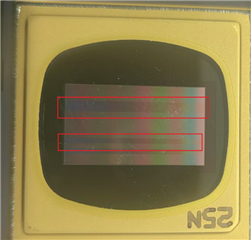
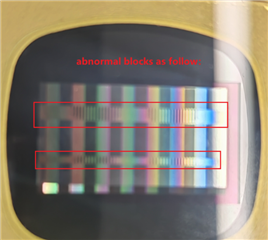
After powering on and completing initialization, approximately three blocks are malfunctioning, as shown in Picture1. These blocks do not behave as expected when displaying images on the DMD, as illustrated in Picture2. We monitored the rst_active signal and observed a 4.5 µs pulse, indicating it is functioning correctly. However, when switching images, these blocks still fail to respond.
Setting the pwr_float signal to low and measuring the AC17 pin of the DLPC410 on the PCB showed a high-level signal. Under normal circumstances, it should be floating, but there is no change in the DMD.
Could you provide any troubleshooting suggestions?
thank you very much!

  • Hello Qiuyan,

    The very latest version is in fact version 0.   There were some minor timing improvements and a reset voltage adjustment for the DLP650LNIR DMD.  So that is good that it is reporting "0".

    The horizontal blocks not working correctly suggests that there is poor contact on the MBRT lines for those three blocks.  If you are using the same flex cables that the TI EVM uses, then the pads and pins should be inspected for any debris and cleaned (pads with Isopropyl alcohol) and the pins with a clean brush.  If not using the same style flex cables, the connections should be reseated and checked.

    The fact that setting power_float low does not AC17 low suggests there is something wrong in the circuitry (bad contact or solder or via, etc .  . .

    Fizix

  • Hi, Fizix:
    We tested the MBRST signal at the output of the DLPA200. When the wdt_enable signal is enabled (wdt_signal=0), the image displays correctly (provided that we wait for 10 seconds for the watchdog to generate a global reset command), and each MBRST signal has an output. However, when the wdt_enable signal is disabled (wdt_signal=1) and we use the blkad and blkmd signals to generate an MCP, only output00 (pin22) of the MBRST has an output.

    What debugging methods can we use next?

  • Hello Qiuyan,

    Are you generating a global MCP?  Once you have set the BLKMD and BLKAD are you sending NOOPs?  This sounds like there is an input missing,

    Please try sending a global reset for a test.  Clearly data is reaching the DMD since it displays with the watchdog timer.

    Fizix

  • Hello Fizix,
         We tested the connection between our FPGA and V5(DLPC410).Now I can program the V5 by the JTAG,So I can monitor those signals from my FPGA at the V5 end.In our FPGA, I generate a PWM signal on every pin(including row_ad,row_md,blk_ad,blk_md) connected to the V5.And I found that some signals has not any variation as follow:

    Can this phenomenon indicate a problem with the hardware connection?

  • Hello Fizix,
            As the picture shown at last thread,we found that blkad[1],blkad[3],blkmd[0] has not any variation.
    And I have traversed the entire list(list 14 in dlpc410 datasheet) of commands,we set the BLKMD and BLKAD generate MCP(follow closely behind sending NO-OPs).Only the commands in the red box in the following image can be executed correctly.This test proves that blkad [0], blkad [1], blkmd [0] are fixed values of 0, regardless of how they are set.And i have try sending a global reset for a test,The result is consistent with setting blkad=0 and blkmd=2'b10,only the micro mirror of block 0 has flipped.


  • Hello Quiyan,

    As I understand it, you have inserted a bit file that sends a signal that is toggling on these lines, but see not response at the other end of that signal interface.  If that is correct then you have a bad trace/connection.  Until that is fixed I don't see how to proceed.

    Also if you send a global reset you must send continuous NOOPs for the next 13 us.

    Fizix