This thread has been locked.

If you have a related question, please click the "Ask a related question" button in the top right corner. The newly created question will be automatically linked to this question.

DLPC3478: FLASH written operation failed

Part Number: DLPC3478
Other Parts Discussed in Thread: DLP3010LC, , DLPA3000, DLPC3470

Tool/software:

Hello, TI team

I’m now debugging my own board designed with DLPC3478, DLPA3000 and DLP3010LC.

I burned the FW of “FWSel_DLPC3478_DLPA3000_AC_pm1_i2c0x36_v9p2p0.img” to the FLASH “W25Q32JWSSIQ” which attached to DLPC3478.

The boot up process is OK. After that LEDs light out a default splash picture with DLP logo.

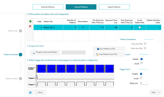
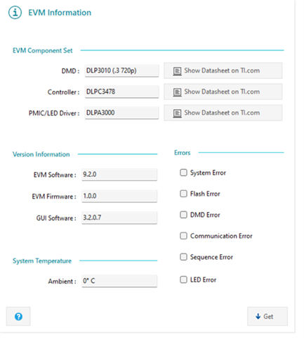
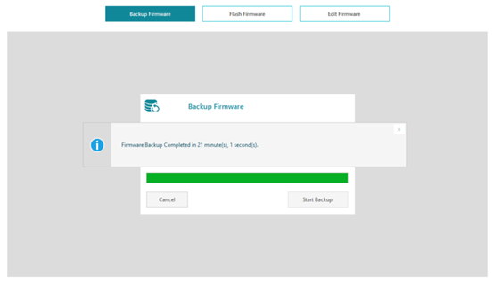
I use “DLP EVM GUI 3.2.0.7” to debug the board by connecting to the I2C port of DLPC3478. Most of the functions are normal, such as test pattern setting in “Display” menu. And Backup Firmware in “Firmware” menu is good, I get the backup file and compare to the origin I burned before, they are of the same.

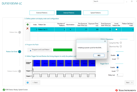
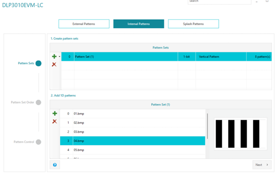
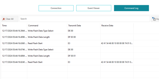
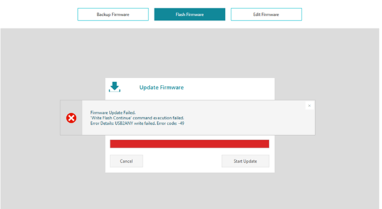
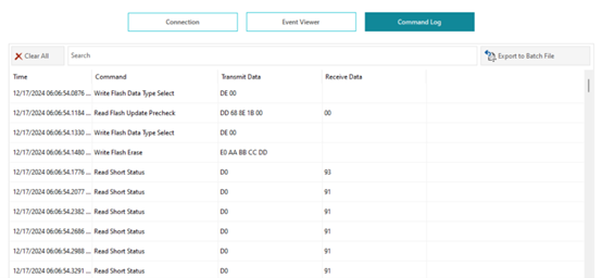
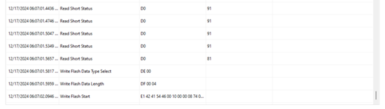
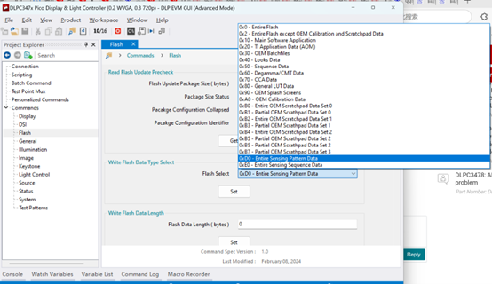
Base on the above operation, I believe the hardware is good. However, when I try to “Program and Load Pattern” in the “Internal Patterns” menu. It failed. The same error happened in the operation of “Flash Firmware”. After that, I reboot the board, the FW has been crashed, I think at least the Flash has been erased. So I had to burn the FW again, and the board become fine.

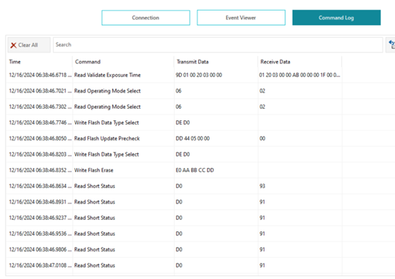
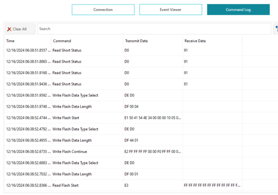
The following are some screenshots of my steps.

Please help me to find out the problems.

Thanks & Regards

Haoyang


  • Hello Haoyang,

    Could you also share the Pattern Sets page? What are the patterns you've added to the pattern sets? These should only be the type of pattern you've selected when creating the pattern set itself.

    Best,

    Aaron

  • Hello Aaron,

    Thanks for your reply.

    The following screenshots show my internal mode setting. There is one set which including 8 patterns. Meanwhile the exposure and dark time paras are set. But the error occurs when I click the “Program and Load Pattern” button, it takes several seconds running and pops out a small window “Initiating a power cycle for EVM..”.

    After the failure above, I check the command log, the final command reading out the data attempt to write into FLASH, it is all FFs. It seems that the data being not written successfully.

    Please help me to analyze.

    Thanks & Regards

    Haoyang Jiang

  • Hello Aaron,

    More Info., As I mention if the first E-mail, backup FW in the GUI works fine even though it will take about 20mins in my 32Mbit FLASH. The output file has been compared is identical to the original one. But the Flash FW function fails, the FLASH has been erased and no correct data inside. So DLCP3478 could not boot up. There are some screenshots.

    I’m wondering if the DPCL3478 will check the FLASH ID? Only the valid ID that can be used. The FLASH mounted on board is W25Q32JWSSIQ, 1.8V IO and 32Mbit. Only the voltage is different from the reference design.

    By far I have no idea now Frowning2

    Thanks & Regards

    Haoyang Jiang


  • Hello Haoyang,

    Thank you for all the images! It really helps me understand what's happening here.

    I am going to reach out to my team who owns the tool to further understand what the error code is saying here.

    I'm sorry for the delay but please give me or them a couple days to return input on your issue.

    Thank you!

    Aaron

  • Hello Aaron,

    Thanks for the support. I will be patient to waiting for your team's feedback.

    Thanks & Regards

    Haoyang Jiang

  • Hello Aaron,

    I keep trying. I found that “Program and Load Pattern” function may corrupt the content of system boot up area in FLASH. But the splash images are still good. After running “Program and Load Pattern”, without reboot the board, I try other functions like changing splash image and test pattern, it works fine. In these processes, DLPC3478 will read the data from the FLASH.

    Hence my idea is “Program and Load Pattern” damaging the boot up related data in FLASH, but not all the other data, at least the splash image data is OK.

    Are there some constrains for the GUI and FLASH?


    Thanks & Regards

    Haoyang Jiang


  • Hello Haoyang,

    If the boot related data in Flash was damaged you would need to reprogram the Bootloader image into this which is not necessary.

    I'll have to hear back from my team about this as well. I'm thinking the GUI may be restricting this or possibly timing out, but that is just a hunch.

    You might consider bypassing the GUI and send direct commands through the API or your own controller to send I2C commands to test this.

    Best,

    Aaron

  • Hello Aaron,

    The GUI is quite convenient in debugging. I really want to try it out. In the command list, before programming into the FLASH, "Read Flash Update Precheck" is passed, it means that the FLASH space is enough for the data ready to be written. All the steps seams OK except the final command "Read Flash Start", the output content is all FFs.

    So the size of Flash should be enough. How about the SPI communication speed? Could it be config to lower down? I check it by oscilloscope, the CLK of SPI is about 30MHz.

    Thank you.

    Haoyang Jiang

  • Hello Aaron,

    One more Info., in the GUI Advanced Mode, "Write Flash Data Type Select" has more paras such as 0xD0-Entire Sensing Pattern Data. However in the "Programmer’s Guide" DLPC3470 and DLPC3478 Software Programmer's Guide, the file name is dlpu075b.pdf, in the page 82, there is a paras table which has fewer paras and no 0xD0. I think it's strange. Why? Am I missing something? The following are two screenshots to be compared.

    Thank you.

    Haoyang Jiang

  • Hello Haoyang,

    Can you help me in understanding the following things.

    1. How are you flashing the FW image after it gets corrupted 

    2. Did you try flashing the FW image from the GUI firmware update.

    3. Could you please share the schematics of the system over personal message

    Regards,
    Kirthi Vignan.

  • Hello Kirthi Vignan,

    1. I use a USB to SPI cable to flash the FLASH again. In my board, there is two SPI masters facing the FLASH, one is DLPC3478, the other is my USB to SPI cable. If I want to flash the whole FW, I plug the cable and set the RESETZ signal low, hence the SPI port of DLPC3478 will be tri-state. The FW can be programed successfully. When the system in normal operation, I just need to take away the cable, DLPC3478 is able to boot up from the FLASH.

    2. Yes, I've tried to flash the FW from GUI. The first step of erasing is done, but the second step is failed immediately. Let me show you the screenshot at the end my E-mail. So the result is unsuccessful.

    3. It's OK.

    Thanks & Regards

    Haoyang Jiang

  • Sorry for forgetting to post the screenshot.

  • Hello Kirthi Vignan,

    I'm not sure having successfully sending the schematics over personal message. It seems that I've sent to Aaron even though I click your ID.

    Thanks

    Haoyang

  • Hello Haoyang,

    Thanks for sharing the schematics. Will reply over private message.

    Regards,
    Kirthi Vignan.