Because of the holidays, TI E2E™ design support forum responses will be delayed from Dec. 25 through Jan. 2. Thank you for your patience.

This thread has been locked.

If you have a related question, please click the "Ask a related question" button in the top right corner. The newly created question will be automatically linked to this question.

Writing and loading solutions over SPI

Other Parts Discussed in Thread: DLPC200

Hello!

I'm working with the DLPC200 via SPI, and so far I've got robust communication with the DLP; I'm able to query version numbers, change the image order LUT, etc. Where I'm stuck is in loading a solution from the parallel flash that I've written (all via SPI).

I'm able to write a 0x138000 byte solution binary file consisting on a single 8bpp image compiled using the X3 Control Software to the parallel flash using the low level 'Parallel Flash Download' commands (section 7.4.2 in the SPI Slave Interface Specification document). The response to the final packet indicates success, although it is different than the expected low level packet response (section 7), and appears to mention the number of bytes written.

I am loading the parallel flash starting at 0x00000000. When I attempt to load the solution from 0x00000000 using LoadSolutionFromFlash (section 6.50), bit 6 of Data[0] in the response (section 6) is set. Using GetExtendedPktFailReason (section 6.1), code 0x0006 is returned, indicating the solution offset address is invalid.

When I tried loading the parallel flash starting at 0x00001000, LoadSolutionFromFlash (using address 0x00001000) still fails, but GetExtendedPktFailReason gives code 0x0007, indicating that the flash is not programmed.

Before writing the flash, I issue a Parallel Flash Erase (section 7.5.1) command, to erase the region from 0x00000000 to 0x01000000. The response indicates success.

Before loading the solution from the flash, I issue a WriteImageOrderLUT (section 6.14) command to only display image 0, in case the DLP has trouble when non-existant images are referenced in the Image Order. The response indicates success.

Is there anything I'm doing incorrectly, or not doing?

Thanks!

-Matt

  • Hello Matt,

    Basically your approach is correct however there are some minor corrections required in your steps. Have provided them below -

    Before loading the solution from the flash, I issue a WriteImageOrderLUT (section 6.14) command to only display image 0, in case the DLP has trouble when non-existant images are referenced in the Image Order. The response indicates success.

    [Sanjeev] You don't need to do it explicitly, the flash solution binary file will have both 8bpp image plus the BatchFile instructions embedded in it. So just issuing the LoadSolutionFromFlash you should get the image displayed.

    I am loading the parallel flash starting at 0x00000000. When I attempt to load the solution from 0x00000000 using LoadSolutionFromFlash (section 6.50), bit 6 of Data[0] in the response (section 6) is set. Using GetExtendedPktFailReason (section 6.1), code 0x0006 is returned, indicating the solution offset address is invalid.

    When I tried loading the parallel flash starting at 0x00001000, LoadSolutionFromFlash (using address 0x00001000) still fails, but GetExtendedPktFailReason gives code 0x0007, indicating that the flash is not programmed.

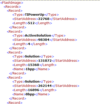
    [Sanjeev] When you build solution binary, there is an .xml file created along with it. If you open and read the XML file, you will find the Solution address, which you need to refer in the LoadSolutionFromFlash command. LoadingSolutionFrom flash and the xml topic is referred in this thread http://e2e.ti.com/support/dlp__mems_micro-electro-mechanical_systems/f/387/t/188164.aspx

    Regards,

    Sanjeev


  • Sanjeev-

    I applied your suggestions and it worked; a single image solution and a six image solution both wrote to flash and loaded properly. Thanks for your help!

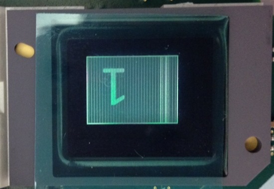
    Unfortunately with both the single image and six image solutions, the images that are displayed are corrupted and offset slightly.

    Here is the image used in the solution:

    Original Image


    And here is a picture of the DMD mirror displaying the image:

    DLP displayed image 

    When displaying the six images, each image is off-center in the exact same way, and the corrupt region varies per image but follows the same general 'two bars' pattern. This same image loaded using the X3 Control GUI over USB on a demo board displays properly.

    Is there something I am doing wrong? I am loading the solution using this tag in the .xml file per the thread you referenced:

    - <Record>
    <Type>Solution</Type>
    <StartAddress>131072</StartAddress>
    <Length>17920</Length>
    <Name>AllImages</Name>
    </Record>
     
    The response to the LoadSolutionFromFlash command reports success.
     
    Thanks again,
    -Matt


  • Hi Matt,

    In the xml file there is something called as ACTIVE solution, which points to default solution to be loaded on power up. So, after you power-on the board, without sending any SPI command the DLPC200 should initialize the default solution, is it happening? In this situation also is it displaying image properly or does it have same image offset problem? 

    Regards,

    Sanjeev

  • Hello Sanjeev-

    Simply powering on the board (no external communication with the DLP), the default solution loads and displays images with the same image offset problem. Visually it appears to be the exact same image offset problem as when I use LoadSolutionFromFlash. This is true for both solutions I have built.

    In addition, I used the X3 Control GUI to build and write a six image solution to a demo board over USB; the images displayed correctly. I then took that exact binary file and loaded it over SPI on my board. It showed the same type of image offset problem.

    Any other suggestions/ideas? Thanks again for your help!

    -Matt

  • Hello Matt,

    OK.

    At this point I think while writing from SPI the data is not getting written properly. 

    Refer to DLPC200 SPI specification section 7.5.1 Parallel Flash Erase command, here set CMD3 = 0x00 instead of 0x10. This is for indication to DLPC200 to compute and return the CRC16 value after writing the binary file into Parallel Flash. 

    When this command is received by the DLPC200 i.e., after receiving last packet data for the parallel flash writing basically it will start computing the CRC16 for the payload. 

    Since, the USB is error free communication we hide this option, but definitely for SPI I think it make sense. We'll make this option as OPTIONAL in the DLPC200 SPI document. We'll update the document accordingly.

    Important thing, DLPC200 starts CRC16 computation from offset = 20 the initial 20 bytes contain basic header which are not useful. 

    Note, with the CRC16 enabled, in the response packet DLPC200 will be add two more bytes (i.e., computed CRC16 value).

    So please attach your binary file + the command response received. CRC16.

    Another thing, with CRC16 enabled, the time taken to send back the response by DLPC200 increase as it needs to compute the CRC16.

    Regards,

    Sanjeev

  • Greetings Sanjeev-

    As I mentioned in the my first post, the response received from the final packet of a Parallel Flash Program (section 7.4.2) differs from the low level packet response described in section 7 -- it is 15 bytes long instead of the 9 bytes in the documentation. Changing CMD3 in the Parallel Flash Erase from 0x10 to 0x00 did not change the size of the response.

    Regardless, I changed CMD3 of the Parallel Flash Erase command from 0x10 to 0x00, and then performed the Parallel Flash Program (section 7.4.2). Below is a comparison of the responses with the CMD3 of the Parallel Flash Erase set to 0x10 and 0x00 beforehand.

    Field CMD3=0x10 CMD3=0x00
    CMD1 0x03 0x03
    CMD2 0x06 0x06
    CMD3 0x00 0x00
    CMD4 0x00 0x00
    Len_LSB 0x08 0x08
    Len_MSB 0x00 0x00
    Data[0] 0x00 0x00
    Data[1] 0x00 0x00
    Data[2] 0x00 0x2D
    Data[3] 0x00 0x8D
    Data[4] 0x80 0x80
    Data[5] 0x13 0x13
    Data[6] 0x00 0x00
    Data[7] 0x00 0x00
    Checksum 0x9B 0x55


    I assume Data[2] and Data[3] contain the CRC16 value, in this case 0x2D and 0x8D respectively, although I don't have documentation (yet!) about the order of those bytes. I've been assuming Data[4] and Data[5] are the number of 256 blocks written, since this solution's file size is 0x138000 bytes long.

    I ran both scenarios several times and the responses were the same each time, and the image displayed both after LoadSolutionFromFlash (section 6.50) and a power cycle always showed the same corruption.

    I've attached the solution binary file I wrote as you requested.


    3326.MattsTestProject.lcp.zip

    Thanks!

    -Matt

  • Hi Matt,

    Can you also send me the version info GetDlpControllerSWVersion (0x0025)?

    If possible read the complete version from USB and send. This will be more helpful.

    CRC16 is returned correctly as expected. Actually this information also embedded within the flash image binary file, look at the offset address 19 & 20. In the attached binary file it is 0x8D2D.

    Similarly in flash response Data[2] & Data[3] the CRC16 is returned, note the order is LSB & then MSB so it is matching 0x8D2D.

    This is further complicating the issue, the data seems to be written properly via SPI which we verified via response packet. 

    Can you create full black and full white image solution, then see how the display looks.

    Regards,

    Sanjeev

  • Hello Sanjeev-

    I have found and resolved the image offset problem! After the CRC was determined to be correct I began investigating other aspects of my system and long story short, the DLP was being pulled out of reset too early during boot. By waiting longer, the image offset problem does not appear.

    Thanks again for your help, I believe I now have all of the functionality that I need!

    -Matt

  • Hi Matt,

    This is a good news.

    I am curious to know how did you increase the reset-out time for DLPC200. Please share. 

    Good luck with your work. Feel free to write us back if you need any other help.

    Regards,

    Sanjeev

  • Hi Sanjeev-

    Our system has an FPGA with a soft processor; during boot, the FPGA now holds the DLPC200 in reset (via the /RESET line, pin A14), and the soft processor then takes the DLPC200 out of reset after ~2 seconds.

    We settled on 2 seconds after finding the Power-Up Requirements section of the DLPC200 Data Sheet (page 37).

    Thanks,

    -Matt