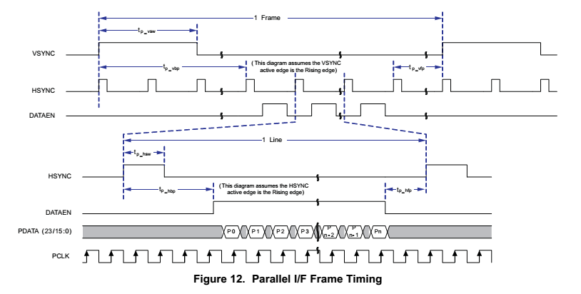
I use FPGA as LCR4500 source. In sequence mode. I choose the trigger mode 0. I enter through LCR4500 of RGB24 mouth. So I transmit timing sequence should trigger mode with programmed instructions on the timing DLPC350 0 same. So, my question is this:
1. Trigger mode 0 mark no time, so I do not know how to set.
2. In addition to the external input vsync, trig_out_1, trig_out_2 these things, we need other external input, such as data enabled, and the synchronous clock if need. And vsync pulse width? And the frequency sequence transmitted?
3. Can you give a similar device ADC Timing Diagram: for example, includes a synchronous clock enable signal, the signal bus, etc.
-
Ask a related question
What is a related question?A related question is a question created from another question. When the related question is created, it will be automatically linked to the original question.


