This thread has been locked.

If you have a related question, please click the "Ask a related question" button in the top right corner. The newly created question will be automatically linked to this question.

DLP6500FYE: DLP6500 EVM Driver Board Pins and Test Points

Part Number: DLP6500FYE
Other Parts Discussed in Thread: DLPC900

Hello there,

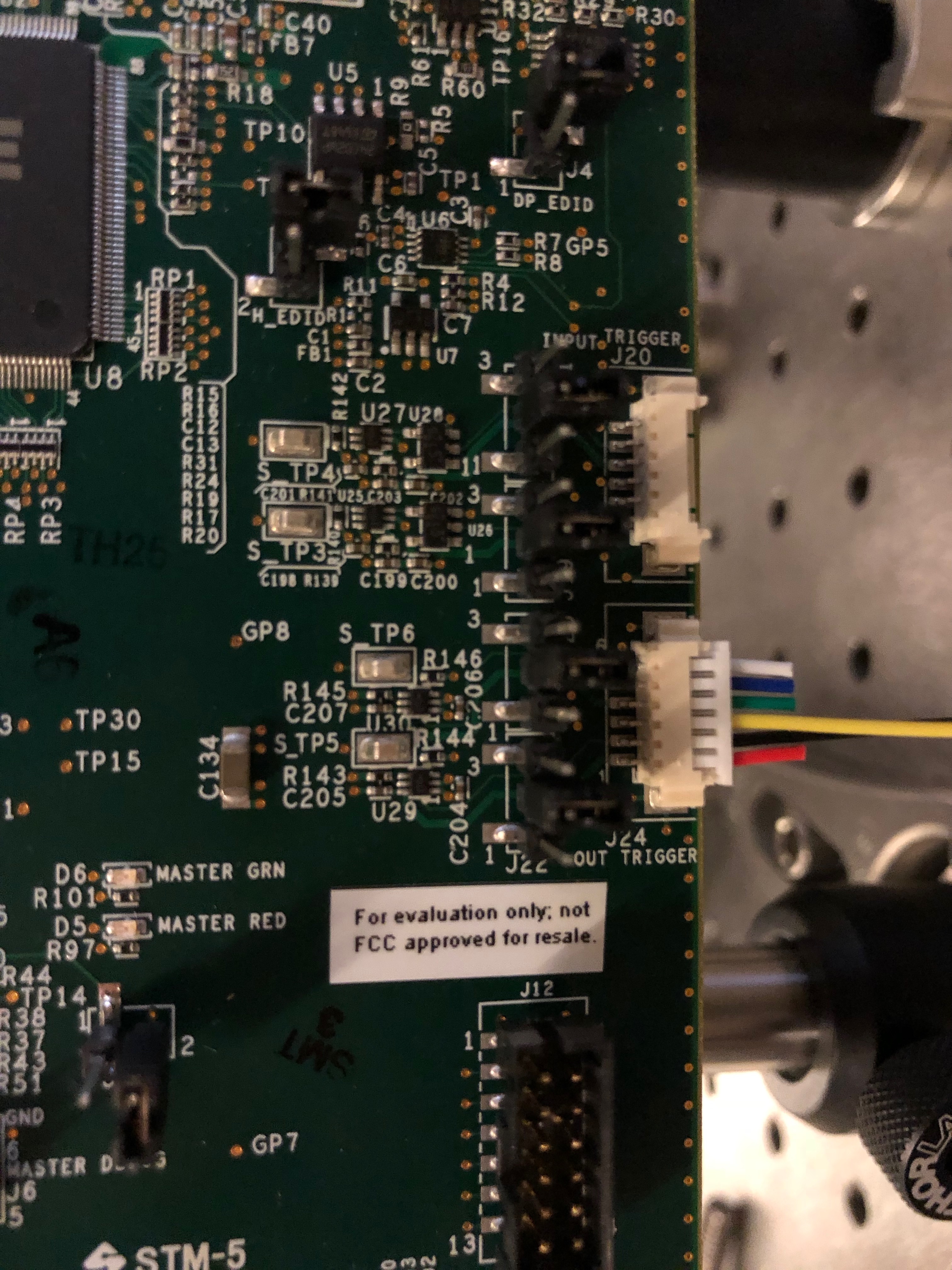
Q1: I am looking for a test point on the DLP6500 EVM board that gives the signal of DADSTRB/AF5 of DLPC900. Do you know where is it?

Q2: Could you perhaps indicate me which pin is for which number for J20 (trigger in) and J24 (trigger out)?

Thank you very much,

Peihang

  • Hi Peihang,

    Schematics and gerbers are at
    www.ti.com/dlp6500-c900ref-hw1_2

    You can also go through EVM User guide at www.ti.com/.../dlpu028c.pdf
    Chapter 4 contains details about J20 and J24.

    DADSTRB is TP14

    Table 4-1. Trigger Input Connector Pins
    J20
    Pin 1 - Trigger In 1 Supply
    Pin 2 - Trigger In 1
    Pin3 - Ground
    Pin4 - Trigger In 2 Supply
    Pin5 -Trigger In 2
    Pin6 - Ground

    J20
    Pin 1 - Trigger Out 1 Supply
    Pin 2 - Trigger Out 1
    Pin3 - Ground
    Pin4 - Trigger Out 2 Supply
    Pin5 -Trigger Out 2
    Pin6 - Ground
  • Hi ykc,

    Thank you very much for your reply. 

    Would you mind quickly indicating me on the diagram attached for J20 and J24 that which pins are pin 1 and 6?

    Also, I am still a bit confused after briefly reading through the evm used guide. In which mode and how can I use the trigger input 1 channel to start displaying my images.

    Best,

    Peihang

  • Peihang,

    Board has marking for pin 1 and pin 6. Anyways pin towards J12 is first pin.
    Section 1.5.2 of EVM user guide depicts this.

    Trigger settings is used in Pattern on Fly or Pre stored pattern mode.