This thread has been locked.

If you have a related question, please click the "Ask a related question" button in the top right corner. The newly created question will be automatically linked to this question.

CCS/DLPC410: RST_ACTIVE is not asserted regularly

Part Number: DLPC410
Other Parts Discussed in Thread: DLP7000, , DLP7000UV

Tool/software: Code Composer Studio

Hi,

Our setup is as followed: (Virtex7, DLPC410, DLP7000)

https://e2e.ti.com/support/dlp/f/94/p/759718/2806469

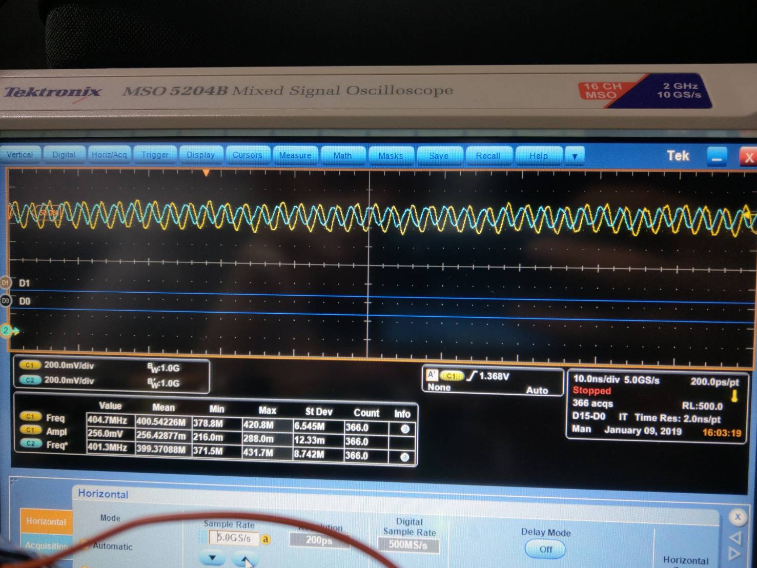
As we have resolved the previous problem, the DLPC410's initialization and calibration go successfully, and we can also retrieve the right DMD_TYPE and VERSION. However, the control outputs somehow couldn't get to the mirror, and I'll list some of our observation below:

1. The RST_ACTIVE stays low even after we output BLK_MD = 11, BLK_AD = 1000, ROW_MD = 00, ROW_AD = 'd0, and other control signals (e.g. wdt_ena, rst2blkz, ns_flip ...) weren't toggled during the output.

2. ECP2_M_TP16 (Clock reset) stays high after initialization. We're not sure if this is normal and what causes this if it is not.

Thanks,

Justin

  • Hi Justin,

    Welcome to DLP section of TI E2E community.
    Please check clocks. It is likely the PLL settings and ranges are different between the 5 and 7 series families.

    -ykc
  • Hi,
    All the PLLs are locked on both APP_FPGA and DLPC410. We also checked the system clock on TP4, and it is a working 200MHz clock.
    Justin
  • Justin,

    What is the timegap between consecutive commands?

    -ykc
  • Hi,

    We followed the datasheet to wait for the micromirror settling time. And as mentioned in the previous post, our code worked before.

    Justin
  • Justin,

    Please see sent command is as per Figure 11 of www.ti.com/.../dlpc410.pdf
    Dvalid is high for 16 clock cycles.

    Also can you provide scope shot of these signals from first dvalid rising to next command dvalid rising.

    -ykc
  • Hi,

    Yes, we kept DVALID high during the whole operation (>16T).

    We could not fetch output ports with ILA, but we can provide our simulation. The interval between the 2 markers is 16T.

    Thanks,

    Justin

  • When you say Reset active is not asserted regularly, is there any pattern to it.
    Like every alternate command is not asserting or it is failing after certain number of commands.

    -ykc
  • Hi,

    I should express it more precisely, the "rst_active" is always low no matter I send a global reset command to DLPC410 or not.

    Thanks,

    Justin
  • Hi Justin,

    Thanks for clarification. Please let me know status of

    ECP2_M_TP28 (pin G10)

    -ykc
  • Hi,

    It's a steady logic low

    Thanks,

    Justin

  • Hi Justin,

    May I know which version of DLPC410 you are using and what dmd_type and version is read? In latest version ECP2_M_TP16(version 7) is expected to be high.

    All the Block mode and block address information will be ignored unless there are valid row cycles taking place. DCLK should continuosly be provided to the DLPC410 and a valid row cycle is when DVALID is asserted for an entire row. If there are no clocks nor DVALID assertion, then no DMD reset will occur.
    There are PLL differences between Virtex 5 and Virtex 7.
    Please double check dclks using oscilloscope.

    -ykc
  • Hi,

    DMD_TYPE:0001, VERSION: 5

    When the PLL and LVSD modules are ready, the DCLK will always be provided. And after the initialization, our DVALID is constantly logic high (we checked the LVDS output using oscilloscope).

    This is our DCLK measurement, is this a valid one?

    In addition, we want to know what is the mechanism of ECP2_M_TP5 (DVALID_A) assertion. Does it indicate directly our DVALID LVDS signal from APP_FPGA, or is it an indication of the validity of the DVALID + DATA  signals? If it is the latter one, and if we measured those signals using an oscilloscope, how can we know if they are valid or not?

    Thanks,

    Justin

  • Hi Justin,

    Dvalid latches the block and mode settings and indicates start of row operation when it is asserted. It should be deasserted after 16 clocks
    Please check Figure 8. DLP7000 / DLP7000UV 2XLVDS DMD Input Data Bus.

    When you say Dvalid is constantly high. You mean right after initialization it stays high?
    Please try keeping it low, adding some delay after init then assert it.

    Please also check Figure 3 of datasheet regarding timing requirements of these signals.

    -ykc

  • Hi Justin,

    DCLK scopeshot you attached is it differential signal ?

    -ykc
  • Hi,

    " It should be deasserted after 16 clocks"

    How long should it be deasserted? We now deasserted it for 2 clocks after asserting it for 16 clocks but the TP5 is still not asserted.

    "Please try keeping it low, adding some delay after init then assert it."

    We now keep it low after init and then assert it.

    "Please also check Figure 3 of datasheet regarding timing requirements of these signals."

    Both of our NS_FLIP and COMP_DATA are constantly logic low.

    "DCLK scopeshot you attached is it differential signal ?"

    We found that the LVDS clock gets well after we inserted a GBUF for the reset pin of the LVDS module. This is our DCLK signal now.

    Thanks,

    Justin

  • Hi Justin,

    Clock certainly look better now. For now keep delay to 32 clocks. Please check skew requirements of Skew, BLK_MD, BLK_AD, ROWMD or ROWAD to DCLKIN in section 8.5.

    -ykc
  • Hi,

    We found that when we deasserted the ARSTZ, the INIT_ACTIVE will only be asserted for 14ms, unlike the 220ms assertion on the datasheet.

    What could possibly cause this, and will this cause any other problem such as the lack of training pattern lasting time?

    Thanks,

    Justin

  • And please we would like to know the mechanism of the ECP2_M_TP5 assertion.

    Thanks a lot,
    Justin

  • Hi Justin,

    When you deassert ARSTZ, training pattern is applied beforehand ?

    In Xilinx FPGAs (due to the construction of the ISERDES and OSERDES cells) a pattern
    of 0010 needs to be applied to the output/transmitting SERDES cells data pins (D1 = 0,
    D2 = 0, D3 = 1, D4 = 0) in order to receive a result of 0100 (Q1 = 0, Q2 = 1, Q3 = 0, Q4 =
    0) at the input/receiving SERDES cell.
    The patterns should be applied on all of the input data and DVALID pins. In this respect,
    the interface is treated as a 17 bit interface with DVALID being the 17th data bit. The
    receiving logic in the DLPC410 will shift the data until the correct pattern is seen at the
    inputs. The SERDES cells align the incoming data with the ½ speed system clock (derived
    from the full speed data clock). This allows DLPC410 to correctly align the DVALID signal
    and the incoming data and will contribute to a more robust interface. It is important that the
    training pattern is applied to the DVALID and data inputs of the DLPC410 before reset to
    the device is deasserted, as training commences immediately on the deassertion of reset.
    The INIT_ACTIVE signal is asserted while the device is held in reset in order to help
    facilitate this behavior.

    After initialization is
    complete, a delay of at least 64 DCLKIN clocks (on all input data buses being used) should be observed before
    the first DVALID is asserted on those data buses to ensure a clean start up process.

    -ykc
  • I checked the D4100 kit which has Virtex 5 and I can see init active asserting for 237ms. After this atleast 64 clks delay is needed.
    During training patterns no signal should be applied on row, block pins.

    -ykc
  • Hi Justin,

    Is there any update on debug?
    FYI I am working on getting details of test points. Looks like there is some discrepancy in datasheet information for these signals.

    -ykc
  • Hi jkc,

    We've been working on how to make DVALID TP assert. And we've confirmed two things as below

    1. Our code works properly on the DDC4100, which means that our code meets the operation sequence of DLPC410.

    After that, we ported this code to the custom board. The only difference between these two projects is the pin assignment file. Still, it doesn't work on the custom board.

    2. Our board contractor did give us a basic working binary code for the board, and this code can demonstrate on the DMD mirror properly. However, we need to port our own code to this platform.

    Since we confirmed that our code isn't the problem of the operation sequence (from initialization to continuous row operation).

    Can you help us to find where the essential problem is? we can provide more information if u need.

    BRs,

    Justin

  • Hi Justin,

    Please provide me logic analyzer capture of all data for these signals right from reset release. First problem is training pattern itself. It should take around 237ms as seen on D4100 kit.

    DCLKA
    DVALIDA
    DCLKB
    DVALIDB

    Also please check
    COMP_DATA
    NS_FLIP
    WDT_ENZ
    PWR_FLOAT
    ROWMD[1:0]
    ROWAD[10:0]
    RST2BLKZ
    BLKMD[1:0]
    BLKAD[10:0]
    Load4

    are all held low during training.

    -ykc
  • Hi Justin,

    Haven't heard back from you. Were you able to debug the problem?

    -ykc
  • Hi ykc,

    We found out that it was the problem of signal integrity, and we decided to redesign the board.

    Thanks again for all the help. Have a great day!

    Justin

  • Thanks for update. Signal integrity is common cause of failure most of the times.

    -ykc