


Other Parts Discussed in Thread: DLP2010NIR, DLPC150
NIRscan Nano-aficionados,
To explain the optics and hardware of the DLP NIRscan Nano, I have disassembled one of our early units manufactured by Coretronic. Note that any disassembly of the optical engine voids the warranty on the NIRscan Nano system. Note that removing the cover on the optical engine allows dust and smudges to collect on the optics affecting its performance. Also, the removing the cover might move the optics, slit, and detector out of alignment requiring factory realignment and recalibration. Removing the slit, InGaAs detector and DLP2010NIR will require the system to be realigned and recalibrated at the factory.
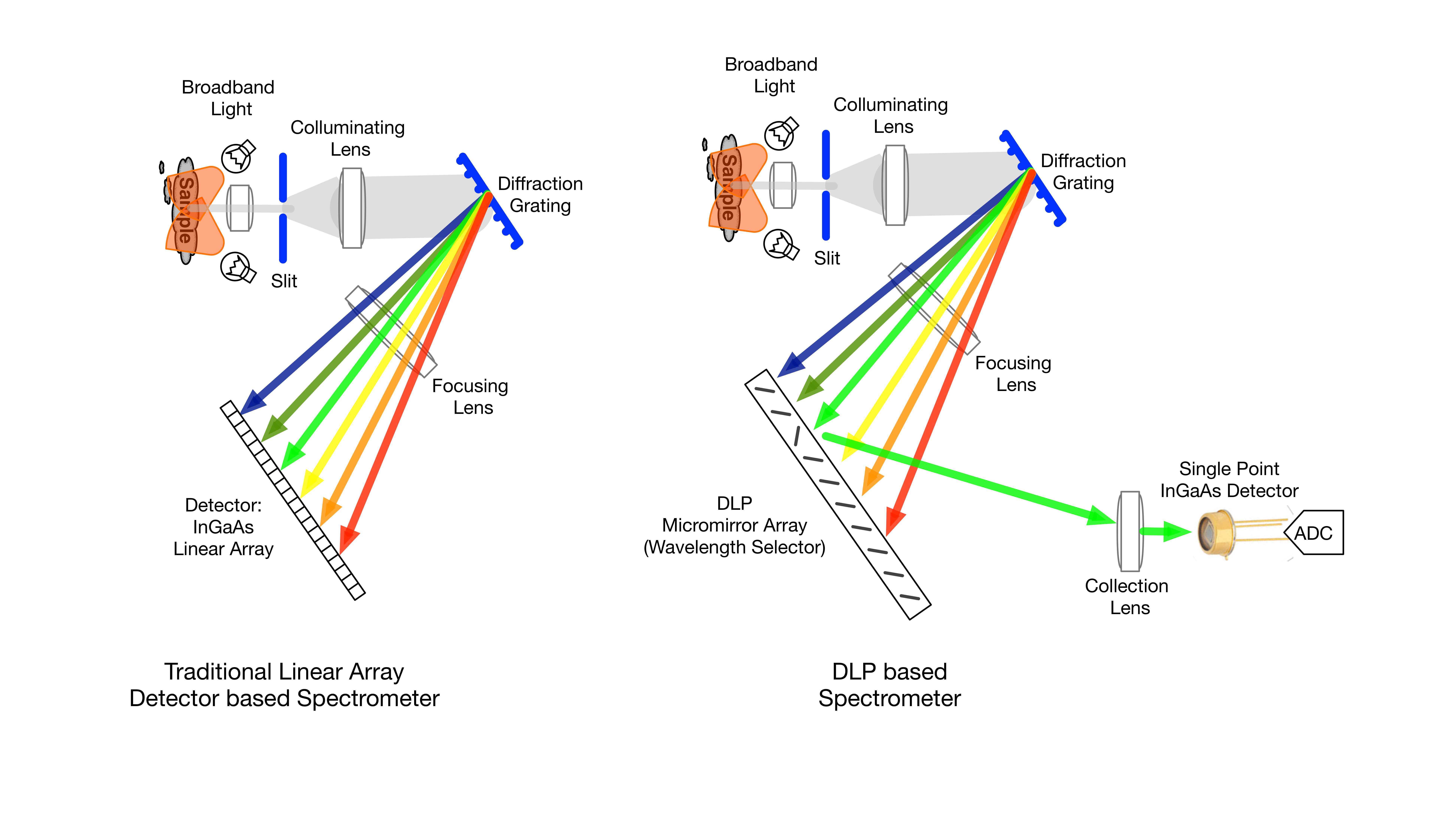
Let me begin with quick overview. DLP based spectrometers replace the traditional linear array detector with a DMD for wavelength selection and a single point detector as shown in the following figure. By sequentially turning on a set of columns pertaining to a particular wavelength of light, the light is directed to the detector and captured. By scanning through a set of columns across the DMD, an absorption spectrum can be computed. Refer to DLP Spectrometer Design Consideration for details on DLP spectrometer implementations.
 DLP technology in Near-Infrared (NIR) spectroscopy provides the following advantages:
- Higher performance through the use of a larger single point 1-mm detector in comparison to a linear array with very small pixels.
- Lower cost system through the use of single element detectors and low cost optics. The high resolution DMD allows custom patterns to compensate for the optical distortion of each individual system.
- Greater signal captured not only because of the larger entendue of the DMD compared to traditional technologies, but also through the use of fast, flexible, and programmable patterns and spectral filters.
- With programmable patterns, a DLP spectrometer can:
- Vary the intensity of light to the detector by controlling the number of pixels in a column.
- Vary the resolution of the system by controlling the width of the columns.
- Use a set of Hadamard patterns that capture multiple wavelengths of light per pattern. Individual wavelengths are then retrieved through a decoding procedure. Each pattern turns on 50% of the DMD pixel at a time, directing much greater signal into the detector than the column scan shown above/
- Use custom spectral filters to select specific wavelengths of interest.
Currently DLP NIRscan Nano software supports variable resolution and Hadamard patterns. Variable intensity and custom spectral filters are not supported. For examples of spectral filters see SPI paper: Latest developments in Texas Instruments DLP near-infrared spectrometers enable the next generation of embedded compact, portable systems by Eric Pruett.
DLP NIRscan Nano has the following major components:
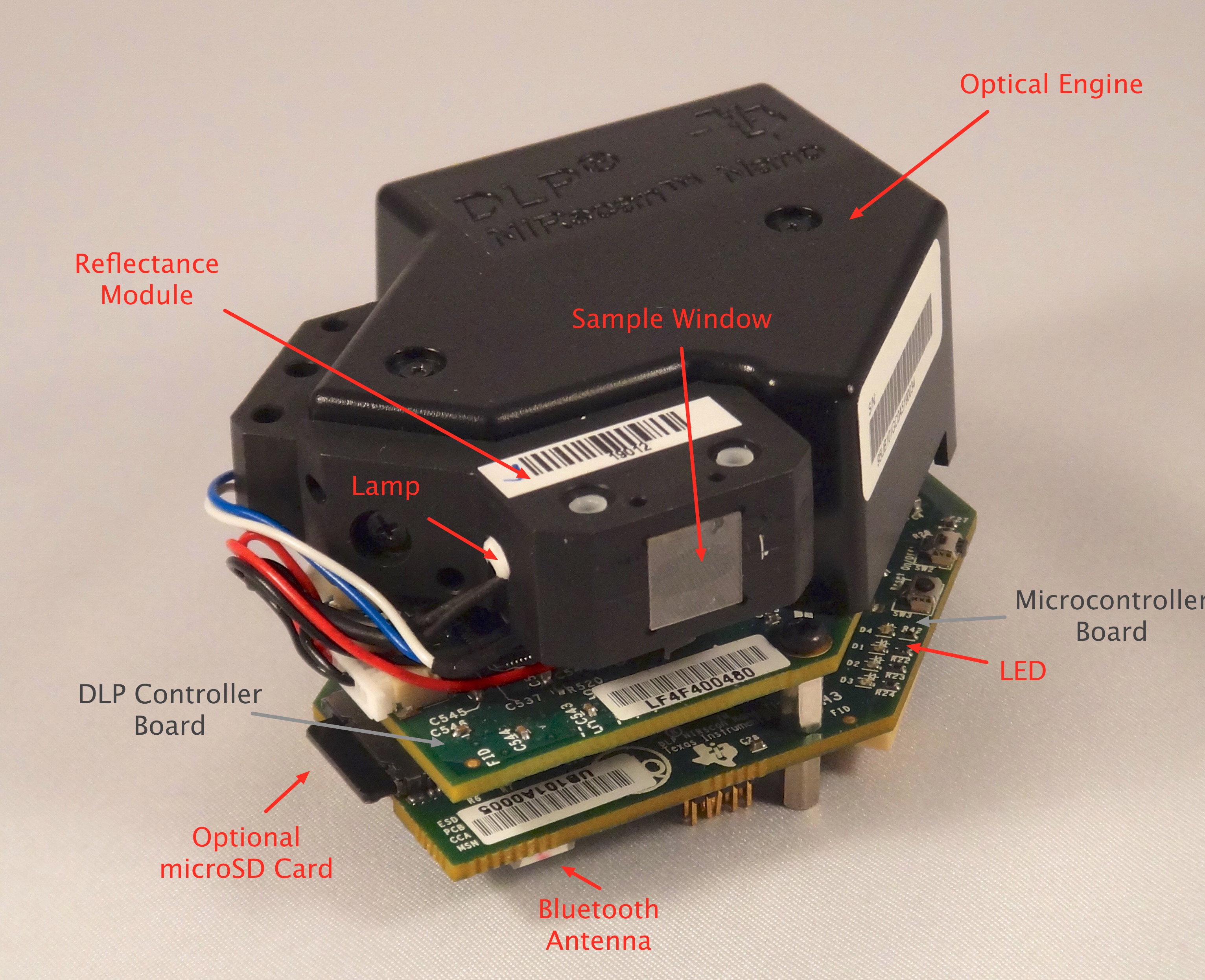
Removing the cover to the optical engine shows the DMD and Detector board that are protected by the cover.
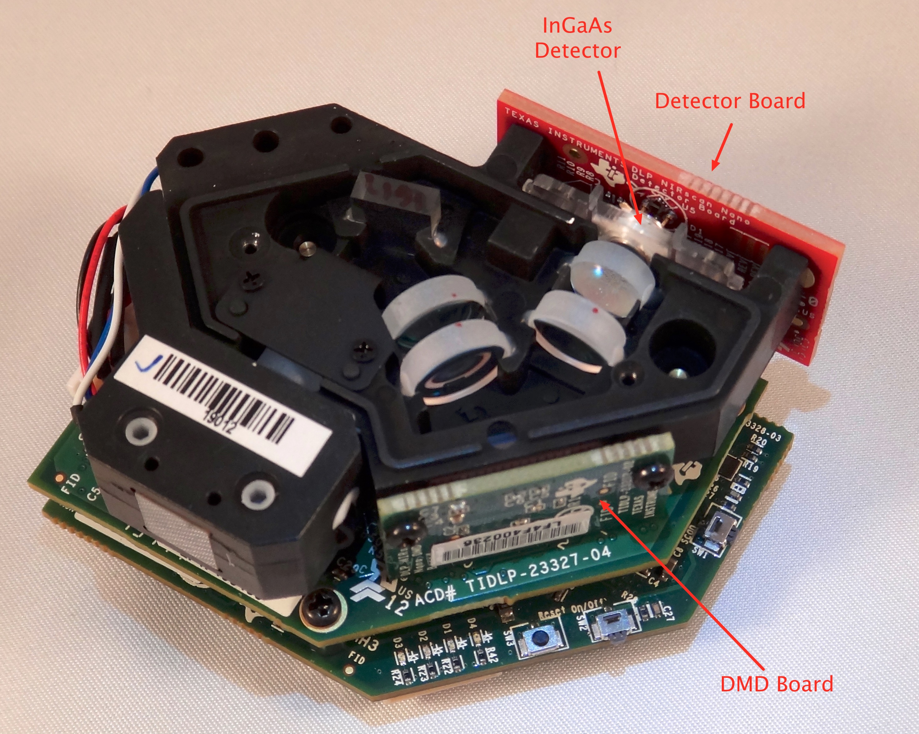
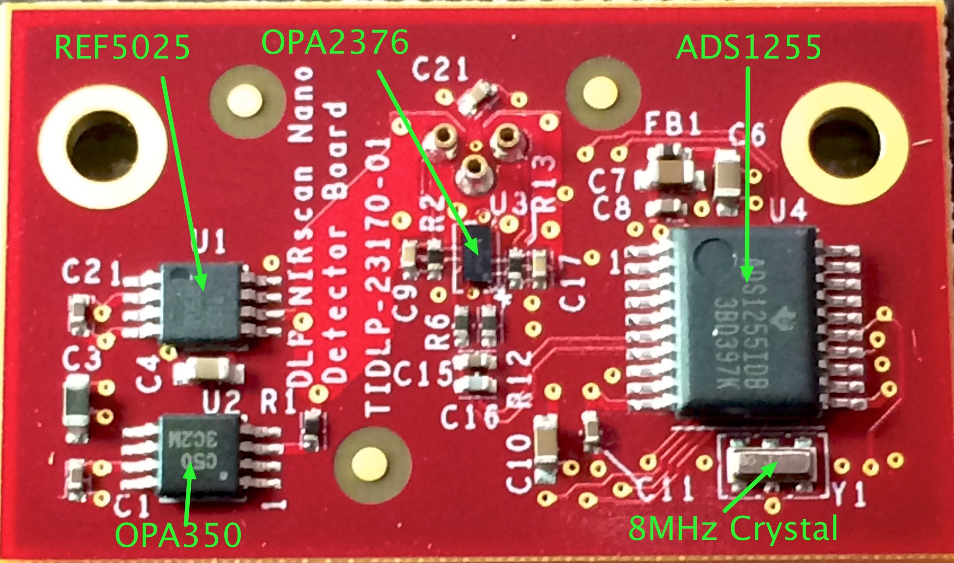
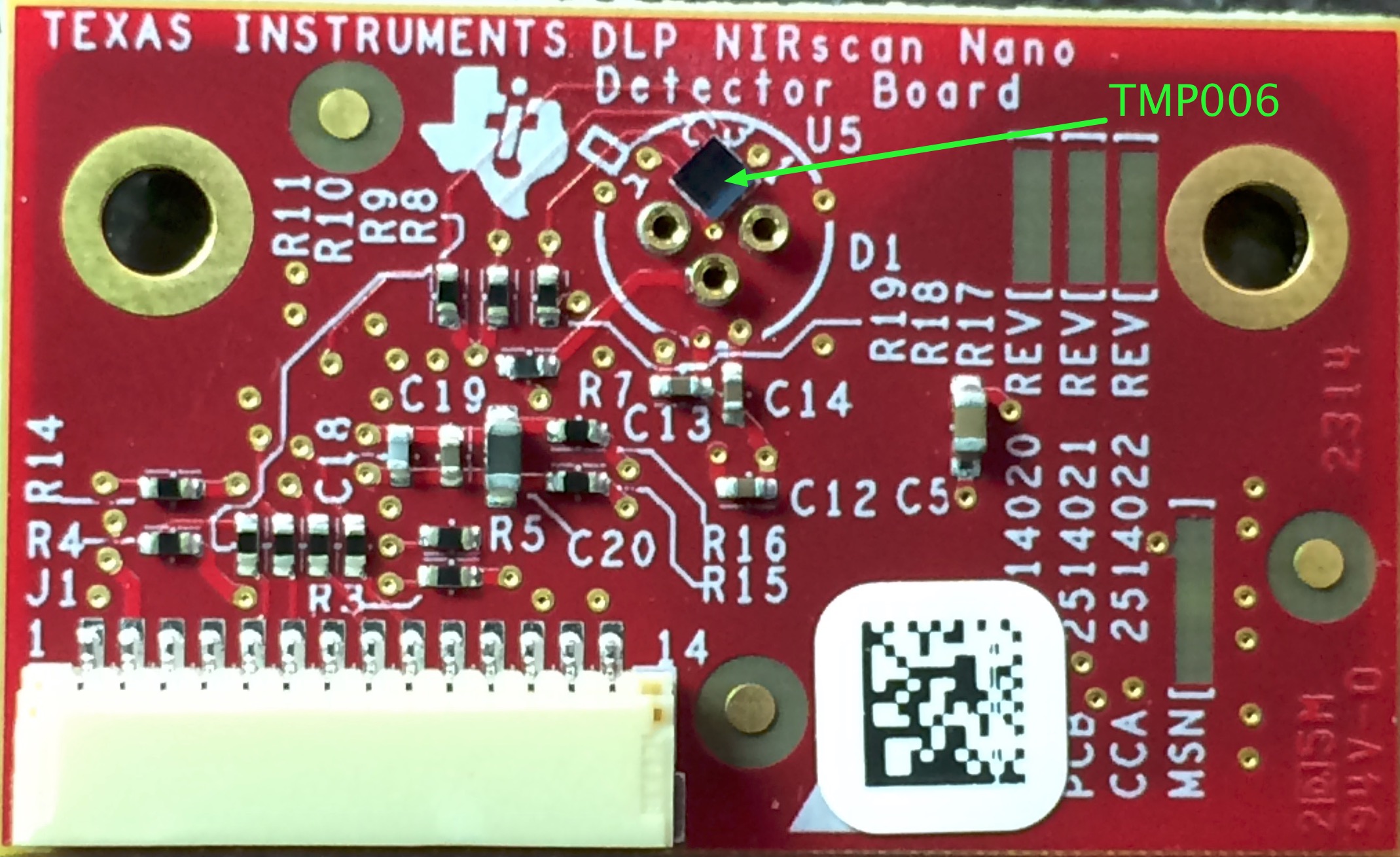
The Detector Board contains the following main components
- 1-mm non-cooled Hamamatsu G12180-010A InGaAs photodiode.
- OPA2376 Transimpedance low-noise amplifier: Amplifies the signal from the InGaAs detector to the ADC.
- ADS1255 ADC: Converts the amplified signal of the InGaAs detector into a 24-bit value for Tiva processing.
- TMP006 thermopile sensor: Measures the InGaAs detector temperature and ambient temperature of the system. These values are captured with each scan.
- REF5025: Low-noise, very-low-drift, precision voltage reference that provides the 2.5-V reference for the transimpedance amplifier and ADC.
- OPA350: High-speed operation amplifier that buffers the 2.5-V reference voltage of the transimpedance amplifier.
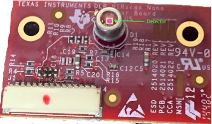
Now with detector installed:
 :
:
Removing the Reflectance module, you can see the slit:

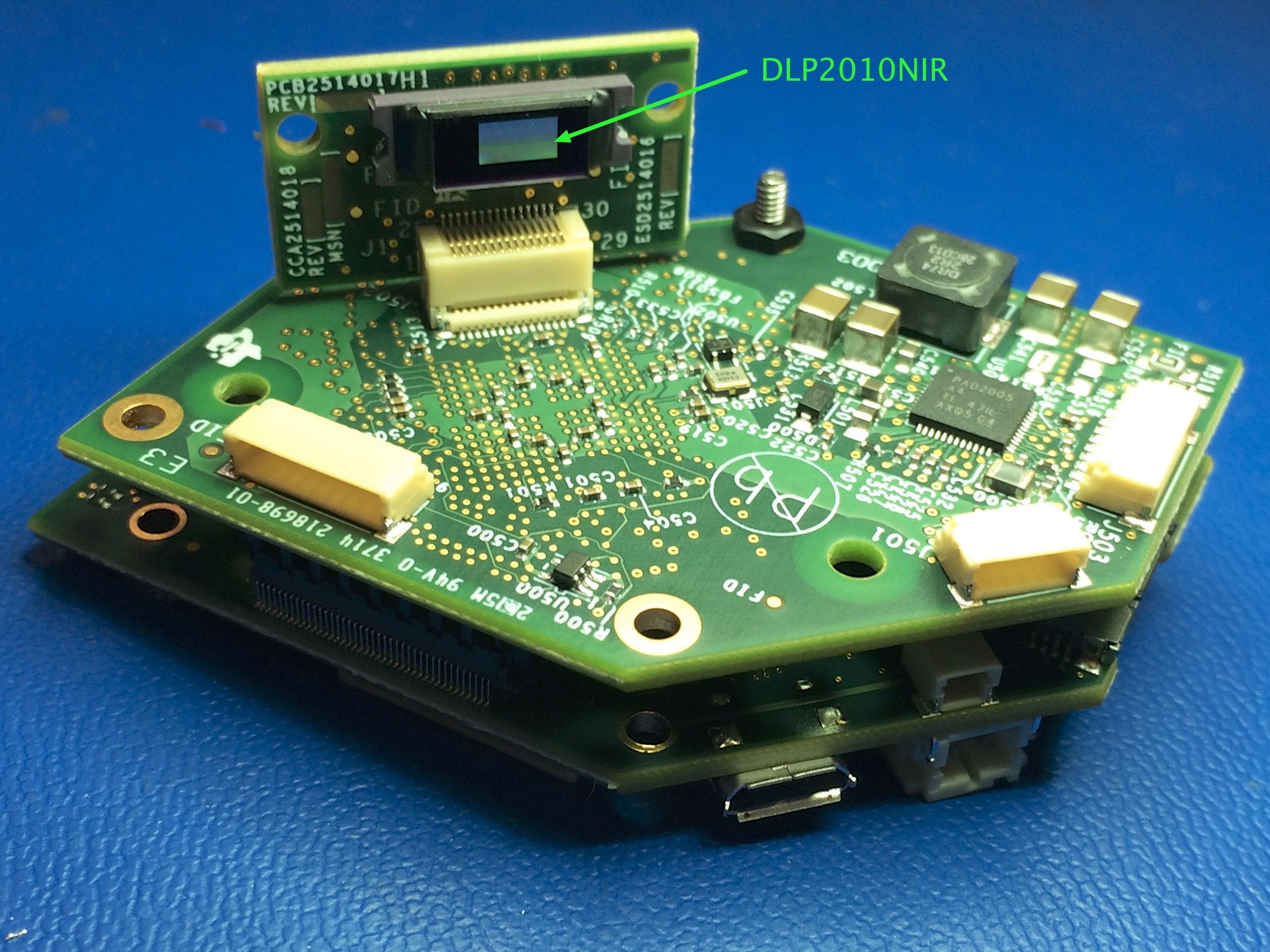
The DMD board just connects the DLP2010NIR to the rest of the system.
Once the cover to the optical engine is removed, you can see the following optical components. The Collimating lenses and Wavepass filter are under a metal aperture that was shown on the previous picture. I have removed the aperture to show all the optics of the system.
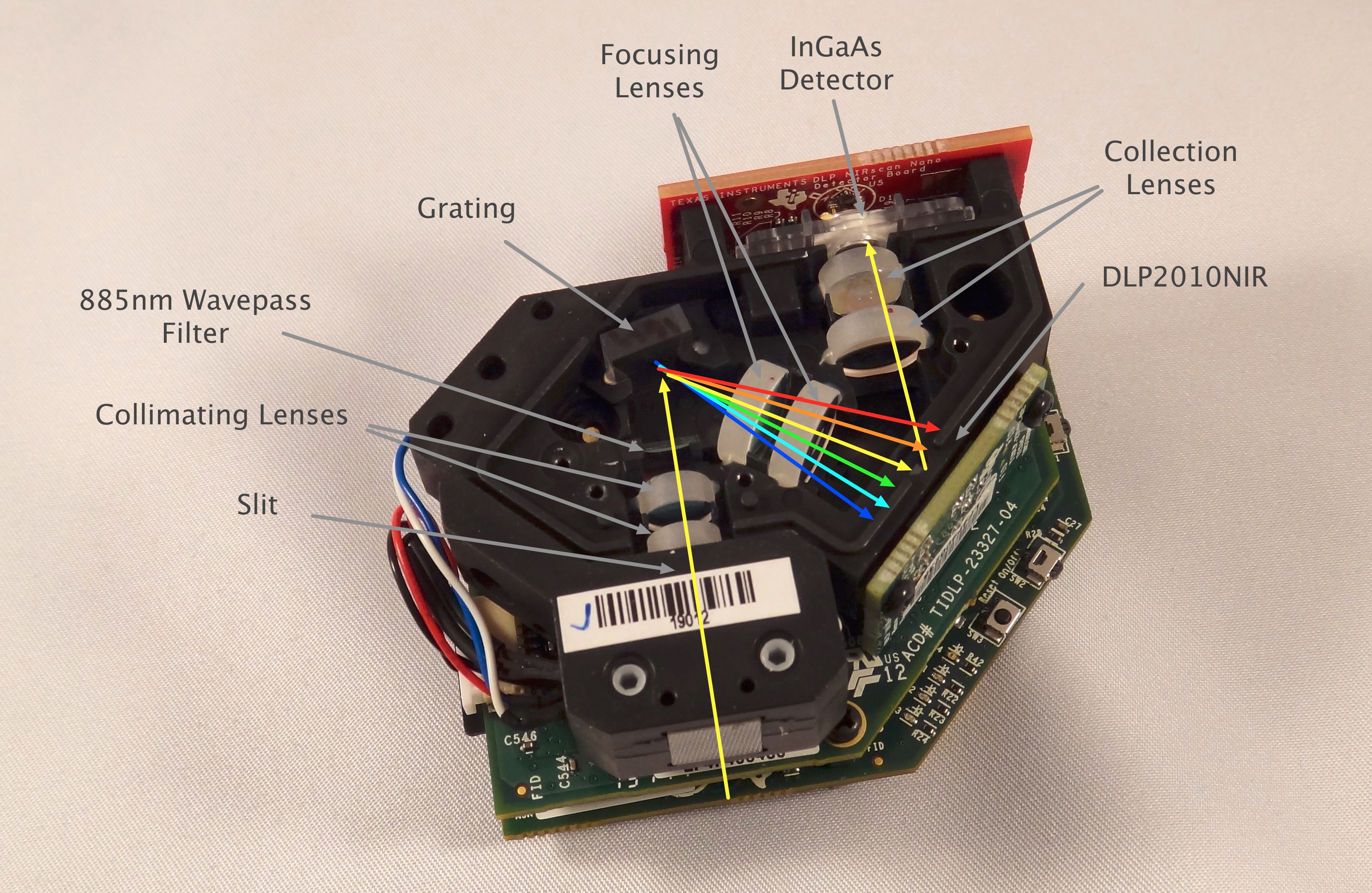
On this figure I have superimposed the input reflected light from the sample (yellow arrow). The light diffusely reflected from the sample is gathered by the Collection lens and focused into the optical engine through the input slit. The slit size is chosen to balance wavelength resolution with SNR of the spectrometer. This spectrometer uses a 25-μm wide by 1.69-mm tall slit. The light that passes through the slit is collimated by the first set of lenses, passes through an 885-nm long wavepass filter, and then strikes a reflective grating. This grating, in combination with the focusing lens, disperses the light into its constituent wavelengths (multi-colored light rays). The focusing lenses form an image of the slit at the DLP2010NIR DMD. Different wavelengths of this slit image are spread horizontally across the DLP2010NIR DMD. The optical system images 900-nm wavelengths to one end of the DMD and 1700-nm to the other end, with all other wavelengths sequentially dispersed in between.
When specific DMD columns are selected as on, or tilted to the +17° position, the energy reflected by the selected columns is directed through the collection optics to the single pixel InGaAs detector (yellow light ray). All other DMD columns selected as off, or tilted to the –17° position, diverts the unselected wavelengths to the bottom of the light engine and away from the detector optical path so as not to interfere with the selected wavelength measurement.
To allow for mechanical tolerances in slit position, grating angle and DMD position, the DLP NIRscan Nano slit image on the DMD is underfilled in the dispersion axis by 10% on each end and overfilled in the orthogonal axis. This results in about (1700 - 900 nm) / ( 854 * 0.8 pixels) = 1.17 nm per pixel on the DMD. During manufacturing a calibration is performed between wavelengths and their column position on the DMD. Since the number of DMD columns is typically not evenly divisible by the number of wavelength groups desired, the DLP NIRscan Nano maintains the column width constant during the scan, but steps through the DMD array by an amount different than the column width. This step amount depends on the desired width and number of patterns (wavelenght points).
The DLP NIRscan Nano reflectance module operates by illuminating the sample under test at an angle so that specular reflections are not collected, while gathering and focusing diffuse reflections to the slit. The illuminating lamps are designated as lens-end lamps because the front end of the glass bulb is formed into a lens that directs more light from the filament to the sample test region. The collection lens gathers light from a 2.5-mm diameter region at the sample window. The size of the collection region was matched to the nominal illumination spot size created by the lens-end lamps. This requires that the sample be placed directly against the sapphire window, where the two angled light source paths intersect the collection vision cone of the lens. If the sample is shifted farther away from the window, the sample may not receive enough illumination for the system to perform an accurate scan. An inside look of the upside down reflectance module is shown below:
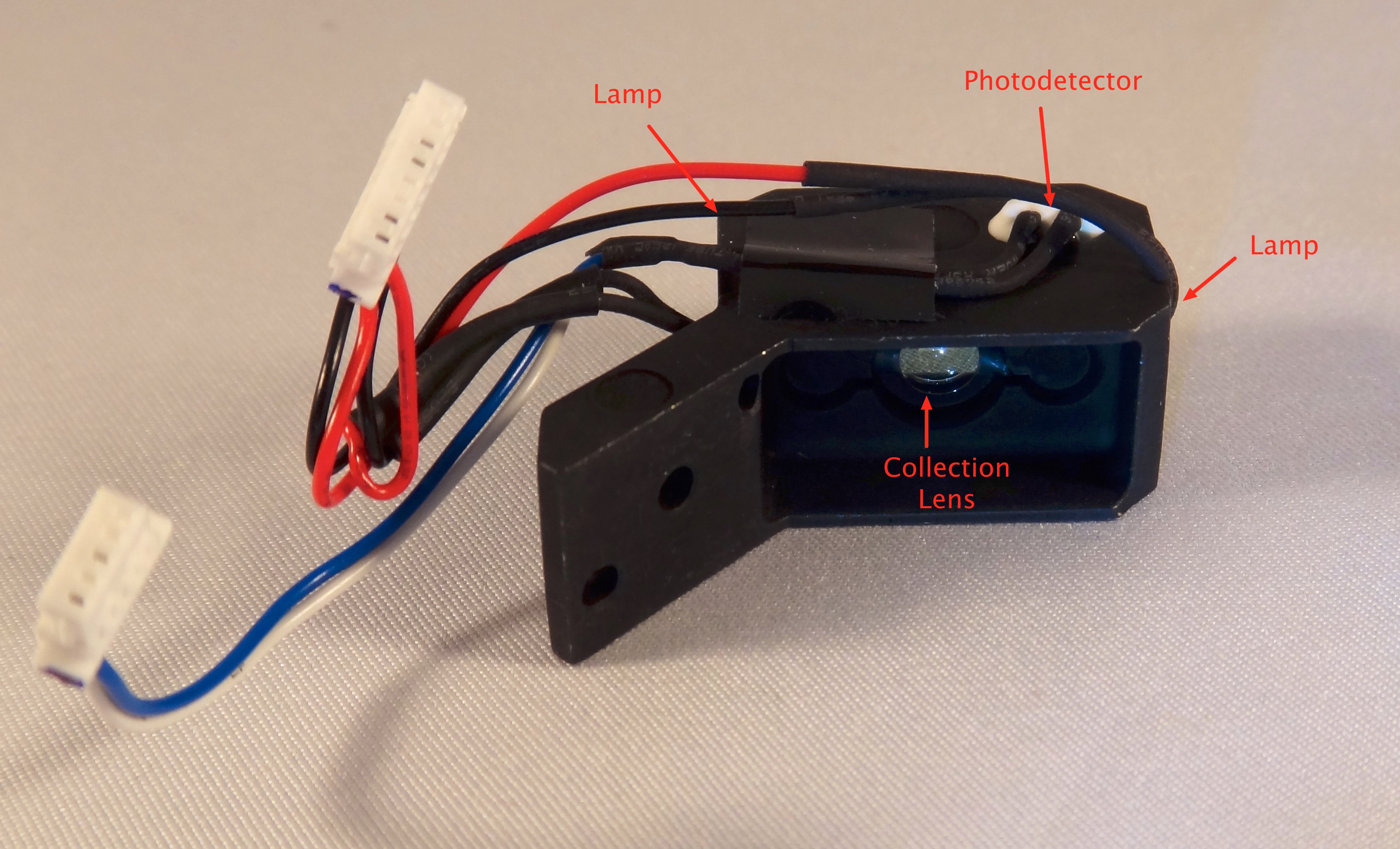
With just the bare optics, you can see the DLP2010NIR from the detector side:

The Microprocessor Board contains the following main components:
- TM4C1297: Cortex-M4 microprocessor operating at 120 MHz with integrated 1MB flash, 256K SRAM, and USB 2.0 interface.
- CC2564MODN: Single chip Bluetooth 4.1 Low Energy subsystem module with on-board antenna.
- bq24250: Single cell Lithium-Ion or Lithium-Polymer battery charger with up to 1-A charge current from USB with an optional battery thermistor to monitor the battery temperature for safe charging.
- TPS63036: High-efficiency buck-boost converter in wafer chip scale package supplies 3.3 V.
- TPS81256: High-efficiency step-up converter in microSIP package supplies 5.0 V for analog circuits.
- HDC1000: Low power, high accuracy temperature and humidity sensor with 14-bit resolution.
The bottom of the Microprocessor Board is shown below:
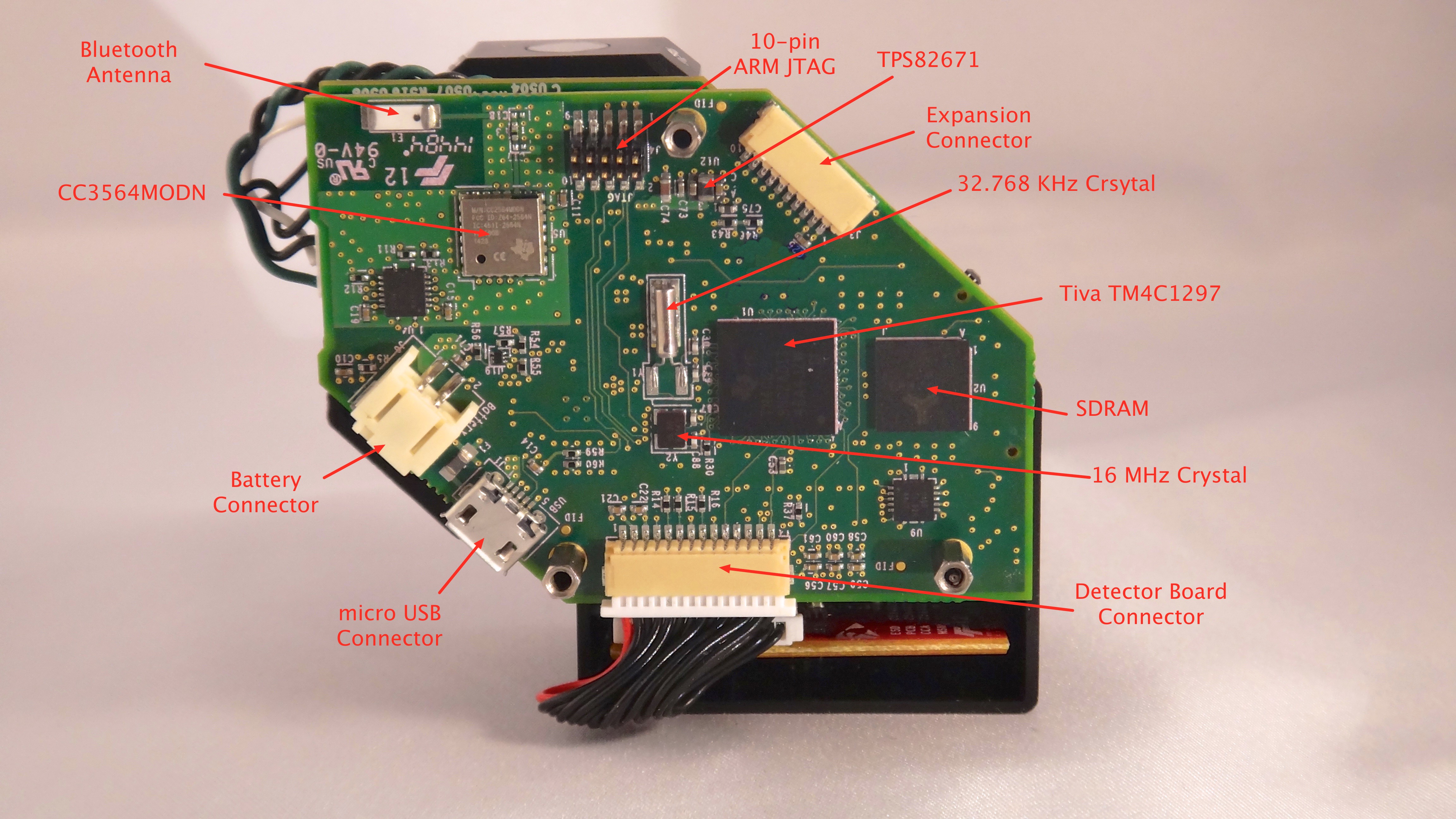
The top of the Microprocessor Board is shown below:

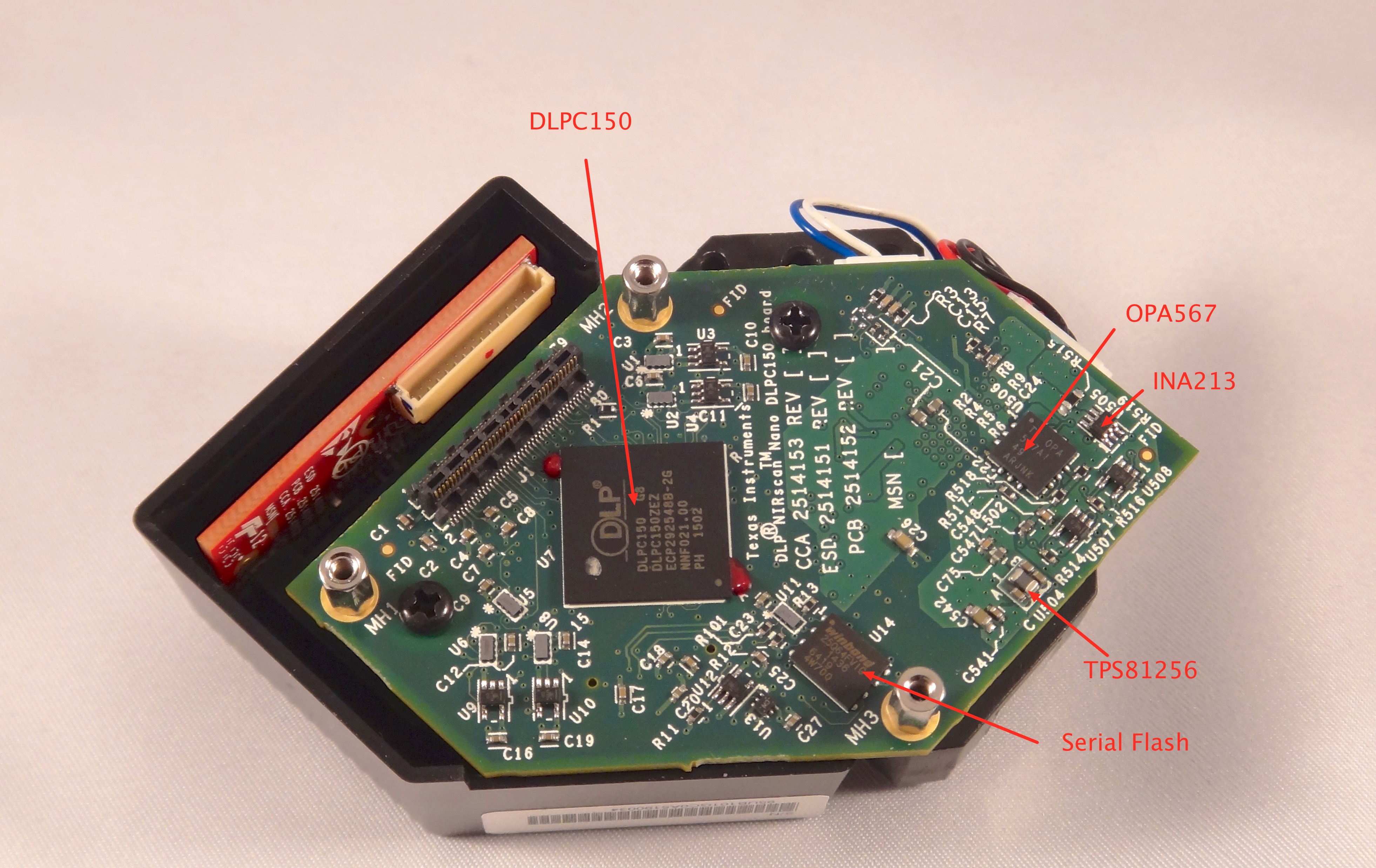
The DLP Controller board contains the following main components:
- DLPC150: DLP digital controller for advanced light control. The TM4C1297 microprocessor in conjunction with the DLPC150 controls individual DLP2010NIR micromirrors to reflect specific wavelengths of light to a single point InGaAs detector.
- PAD2005: DLP power management integrated circuit that powers the DLP 1.8-V, 10-V, 18-V, and –14-V supplies.
- TPS81256: High-efficiency step-up converter in microSIP package supplies 5.0 V for the lamp driver.
- OPA567: 2-A power amplifier that supplies 280-mA lamp current.
- INA213: Voltage output, current-shunt monitor that monitors lamp current.
The bottom of the DLP Controller Board is shown below:
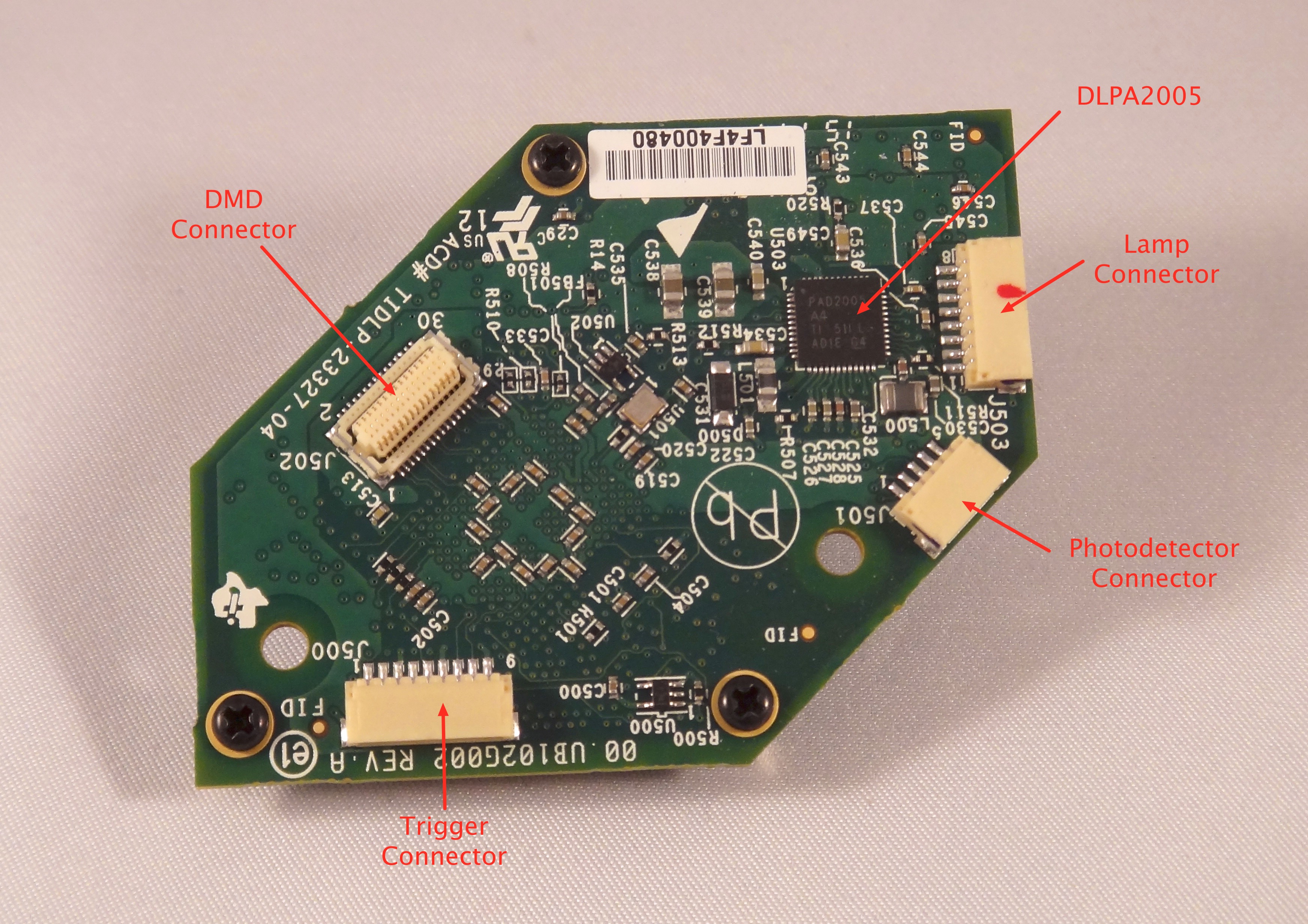
The top of the DLP Controller Board is shown below:
For more information on DLP NIRscan Nano, refer to the DLP NIRscan Nano User's Guide.