This thread has been locked.

If you have a related question, please click the "Ask a related question" button in the top right corner. The newly created question will be automatically linked to this question.

EMIF-16 address mapping?

Another post relating to connecting an FPGA to a C6678 over EMIF-16.  The Keystone EMIF docs (SPRUGZ3A) show several different ways of configuring the interface, eg. for NAND flash versus NOR flash.

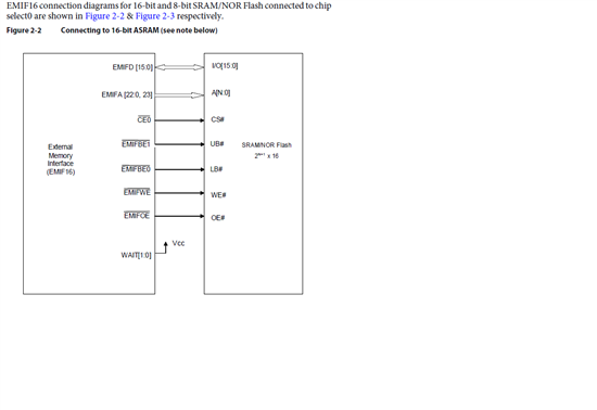
We reasoned that our FPGA was most like NOR flash/ASRAM and started working from Fig 2.2 (p2-4) which show the address lines A[23:0] being wired to NOR device address lines as A[22:0, 23].  There is a note which says

"Note—EMIFA[23:22] behave as address selects. For 16-bit interface, EMIFA23
is connected to address pin A0 of the ASRAM/NOR Flash. For 8-bit interface,
EMIFA[23:22] are connected to address pins A[1:0] of the ASRAM/NOR
Flash."

Except, in our case this doesn't seem to make sense - the address seems to come out "naturally" on A[23:0] without this rearrangement. 

So my question is, what is this A[22:0, 23] business about?  I could understand shifting the address right to omit the irrelevant bit 0, but why shift left and what does A23 have to do with things?  Is there some NOR-flash mode that we should or should not be enabling in order to use the address bus sensibly?

Thanks in advance,

Gordon

  • The EMIF interface in TI components aligns A0 with a 32bit data word.  The addressing is set up like you have a 32bit wide memory device.  If you are reading the first four 32bit locations the addresses presented to the memory devices would be 0x000000, 0x000001, 0x000002, 0x000003.  Each read would return 4 bytes (32bits) of data for a total of 16 bytes of data.  Now assume you only had a 16bit memory device connected to the EMIF interface.  To read the same 16 bytes of data you would have to do eight accesses and the addresses presented to the memory device would be 0x000000, 0x000001, 0x000002, 0x000003, 0x000004, 0x000005, 0x000006, 0x000007.  Remember that the EMIF interface always considers A0 to be a 32bit boundary so the least significant address bit for the extra accesses needed when using a 16bit memory is pulled from the top of the address bits or A23.  If you actually looked directly on the EMIF address pins on the C6678 the above sequence would look like 0x000000, 0x800000, 0x000001, 0x800001, 0x000002, 0x800002, 0x000003, 0x800003. 

    This is significant because of how the compiler will access the external memory.  If your software reads 16 bytes of external memory it will generate the address pattern shown above.  Usually the device you're addressing won't have 23 address bits so If you have not connected A23 to the least significant address bit on you memory or FPGA then you'll end up reading location 0x0000 twice.

  • Bill,

    Thanks for the detailed reply.  That is the behaviour we were seeing, and we had concluded we needed A[22:0,23] << 1 as the address based on a logic analyser on the bus.

    It's nice to have the reason explained though.

    You might consider putting this explanation into the next revision of SPRUGZ3 (f there is one), as several of us read through it when doing this design and none of us picked up that A0 was intended to be 32-bit aligned given that this is only a 16-bit-wide bus.  It's also quite confusing to have called the low-address pin "A23" - out of curiousity, are there any circumstances when it does actually function as address line A23, or is that just not feasible with this design?  Your older parts called it "bank address" or something, that's a bit clearer.  Anyway that's by the by.

    Cheers,

    Gordon

  • Hi Gordan,

    I'll discuss the description with the document owner and see if we can clarify the explanation.  The internal logic that controls the EMIF interface is common for 32bit, 16bit and 8bit EMIF interfaces.  If the C6678 had 32bits of data on the part and these bits were connected to a 32bit memory device then A23 would actually function as the most significant address bit.  Since this is a 16bit data interface A23 will never be used as the MSB of the address bus and will always be connected to A0 of a 16bit memory device or A1 of an 8bit memory device.  There has always been discussion about whether to rename the address bits on parts with an EMIF16 so the present A23 would be named A0 and the present A0 would be named A1, etc but that would be inconsistent with the documentation of other parts.  We've stuck with the convention that A0 is always a 32bit boundary and that A23 and A22 shift if you're using a narrower data bus.