This thread has been locked.

If you have a related question, please click the "Ask a related question" button in the top right corner. The newly created question will be automatically linked to this question.

Keystone 2 EMIF-16 x16 bit NOR

Expert 1800 points
Other Parts Discussed in Thread: OMAP-L138

Hi,

Our aim is to connect 128MB x16 NOR flash to EMIF-16 interface.  

1. Can you please let us know what is the maximum size of 16bit NOR flash that can be interfaced through EMIF-16 interface in Keystone 2?

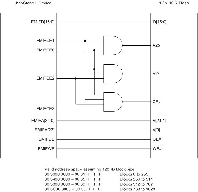
2. As per the documentation, SPRS866E, page no. 93 says that EMIF 16 supports 64M per CE.  

00 3000 0000  -   00 33FF FFFF 64M EMIF16 CE0 EMIF16 CE0 EMIF16 CE0
00 3400 0000  -   00 37FF FFFF 64M EMIF16 CE1 EMIF16 CE1 EMIF16 CE1
00 3800 0000  -   00 3BFF FFFF 64M EMIF16 CE2 EMIF16 CE2 EMIF16 CE2
00 3C00 0000  -   00 3FFF FFFF 64M EMIF16 CE3 EMIF16 CE3 EMIF16 CE3

How can we then interface 128MB flash with 24 EMIF address lines and together with CE0 & CE1?

Thanks

Rams

  • Hi Rams,

    Each chip enable is assigned 64MB of the memory map but only 32MB is addressable if a 16bit data bus is used and only 16MB is addressable if an 8bit data bus is used. If you want to connect a 2Gb NOR flash device with a x16bit data bus, you would only be able to address a quarter of the memory with a chip enable. There are a number of ways that you could solve this issue. You could use all four chip enables and add some decode logic to generate the upper two address bits for you NOR flash. You could also use a couple of GPIOs to drive the upper two addresses and treat the device as a paged memory access. That method wouldn't require an external logic but you would need to handle the paging with software. 

    Regards, Bill

  • Hi Bill,

    Thanks for the response.  We have a 1Gb NOR flash device.   You say that with each chip enable, 32MB is addressable if a 16bit data bus is used and we have to use additional decoding logic to generate the upper two address bits.  Also, inorder to generate the upper two address bits, we should use all four chip enables together with decoding logic.  Is that possible to make use of all chip enables, if we are addressing only 0x30000000 to 0x37FF FFFF?

    1. Can you please show an example usage on how to connect a 1Gb NOR flash device with a x16bit data on EMIF 16 interface with decoding logic for the upper two address bits?

    2. You have also suggested an alternate solution using GPIO lines and paged memory access.  Is there an application note covering page memory access.?  Can you explain this further?

    Thanks

    Rams

  • Hi Bill,

    Could you please respond to the query?

    Thanks

    Rams

  • Hi Rams,

    First let me correct myself. As you pointed out, your 128MB x16 NOR is actually a 1Gb device. It still requires 26 address bits. You will not be able to address all of the memory continuously. If you are using four chips selects than you would be addressing the first 32MB of the address range of each chip select. If you use GPIOs as page addresses then you would only be using the first 32MB of one chip select but you would have to set the GPIOs to address the proper page. Either method will require software to determine which page is currently in use. 

    I don't have examples or app notes for either of the two methods suggested. The first method would require some encoder logic that would translate one of the four chip enables to a two bit address field. This would require some time so additional clocks would have to be added to the setup period to compensate. The second method could be as simple as a direct connection from two GPIO pins to the upper address bits with pull down resistors. Software would have to set the GPIO bits before any EMIF access was made.

    Regards, Bill

  • Hi Bill,

    Thanks for the clarification.  We have connected 1Gbit NOR device to EMIF interface and using all the chip enables to decode A25 and A24 address lines. For this to work, it should be possible to configure the chip selects for this configuration to have contiguous  blocks of 32MB per chip selects.

    CE3 CE2 CE1 CE0 A25 A24
    1 1 1 0 0 0
    1 1 0 1 0 1
    1 0 1 1 1 0
    0 1 1 1 1 1

    Can you please let me know, if there is a way to configure the CE so that 32MB contiguous access can be achieved with each CE?

    Also, I just came across an example usage of EMIF interface on a different TI device.

    http://processors.wiki.ti.com/index.php/Connecting_NOR_Flash_to_OMAP-L138#Hardware_Connection_for_64Mx16_device

    We have the similar decoding logic, but we want to configure each CE to address 32MB contiguous blocks.

    Regards

    Rams

  • Hi Rams,

    I put together a similar diagram for KeyStone II devices, including the addressing I would expect. I put this together quickly so please check my work before you use it. You will also have to compensate for the delay through the gates in your timing. 

    Regards, Bill

  • Hi Bill,

    Thanks for the response.

    This is what we have already done in our custom board assuming that the CEs are configurable.  We want to address 00 3000 0000 - 00 33FF FFFF,  Block 0 to 511 of 128KB block size as contiguous memory.  We do not want to have gaps.  How do we handle the gaps left like 00 31FF FFFF to 00 3400 0000?  Are there already flash drivers in U-boot and kernel to aggregate 4 blocks as one single contiguous memory?

    Or Is there a way to configure the CEs of EMIF interface for desired address ranges? 

    Regards

    Rams

  • Hi Rams,

    The addresses assigned to the CEs are not configurable. You will have gaps between the blocks in your addressing.

    Regards, Bill

  • Hi Bill,

     It is very unfortunate that we cannot configure CEs.  Is there any workaround for this limitation? How can we make use of discrete blocks when we want to address a contiguous block?  Do we have to have a layer above flash drivers in U-Boot and kernel to do mapping to aggregate these discrete blocks to be seen as a single addressable block?  Are such solutions already available with TI?

    Regards

    Rams

  • Hi Rams,

    We've never worked with flash devices that big. The four chip enables were provided to support four separate memory devices. You are breaking new ground so we don't have any example code to support your situation. Since we can't remap the addresses associated with the CE, you'll have to create a handler for your design.

    Regards, Bill

  • Hi Bill,

    Thanks. We got it working.  We were able to concatenate all the regions as single contiguous block.

    Thanks

    Rams

  • Hi Rams,

    That's great to hear. If you have a few extra minute, I would like to know the solution that you implemented.

    Thanks, Bill

  • Hi Bill,

    We already have a solution in U-Boot and linux called MTD Concatenate which will do the job of concatenating the regions into single contiguous block by creating a virtual MTD.  The CFI layer needs minor adaptation to identify the the four 32MB blocks as four individual NOR Chips.  The rest will be handled by MTD driver.  We have tested this in U-boot and Kernel and it works fine.

    Regards

    Rams

  • Hi Rams,

    OK, I understand you methodology. It's always nice when software can overcome the hardware limitations. Thanks for providing your solution to the community. 

    Regards, Bill