This thread has been locked.

If you have a related question, please click the "Ask a related question" button in the top right corner. The newly created question will be automatically linked to this question.

Soldering of TI DS90LV001TLD

Other Parts Discussed in Thread: DS90LV001

Hi,

We have a query about the manufacturability of one of the TI components we use on the majority of our PCB designs and hope the forum might be able to assist us with it. The component in question is the TI  DS90LV001TLD, which is used on most of our PCB designs. While the small form-factor of the WSON package has allowed us create more compact designs, we have struggled with reliably soldering this to our boards during the assembly process. Are there any recommendations on how best to approach the fitting of this package (e.g. solder mask) and any additional notes on layout (e.g. maximum thickness of track entering the pads)?

The package dimensions in the latest datasheet are as follows:


The recommended footprint on the datasheet is as follows:


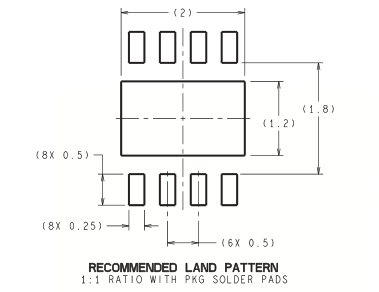
The main thing we've noted on this is that it recommends a “1:1 ratio with PKG solder pads”. Why is it not suitable to increase the pad sizes in the vertical direction (away from the central pad)? We would appreciate any feedback that can be given.

At present we connect ground to the central pad (as suggested in the datasheet). We do this by tracking the ground pin to the central pad – could this cause the package to rotate during solder reflow or is it an acceptable method of routing?

The datasheet was sourced on the TI website at the following location:

http://www.ti.com/lit/ds/symlink/ds90lv001.pdf

Best regards,

Eoin

  • Eoin

    There is a separate application note here: http://www.ti.com/lit/an/snoa401q/snoa401q.pdf which will provide you with a lot of additional information on the Leadless Leadframe Package used by the DS90LV001.

    Mark


  • Hi Mark,

    Many thanks for the response. While that application note is quite detailed, it doesn't appear to address the issues I have, which are: (a) why is a 1:1 pad to footprint ratio specified and (b) can the pad sizes be increased.

    Best regards,

    Eoin

  • Hi Eoin,

    I am a packaging enginner from SVA. DS90LV001 is packaged in a QFN with "lead pullback". As you can see there is a 0.1 mm lead pull back from the body edge. This is the first generation LLP/QFN from NSC. In our early development, we have increased the pad size trying to create a solder fillet as seen in AN-1187 apllicatiopn note. Unfortunately, the solder fillet created is really not a fillet, but the solder is pushed outward to form a solder bump on the extended pad. This pushed out solder will reduce the solder standoff which will degrade the board level reliability.

    Please take a look at page 16 of AN-1187.http://ptg.itg.ti.com/html/packaging_databook.html

    All "No Pullback" will have an extended pad extended outward by 0.2 mm for form a good solder filler.  

    If you have any question, you can call me at (408) 721-5420. Than kyou.

    Regards,