This thread has been locked.

If you have a related question, please click the "Ask a related question" button in the top right corner. The newly created question will be automatically linked to this question.

OMAP-L138: Exit DEEPSLEEP mode and recovery the program

Part Number: OMAPL138B-EP
Other Parts Discussed in Thread: SYSBIOS

Tool/software: Starterware

Dear,

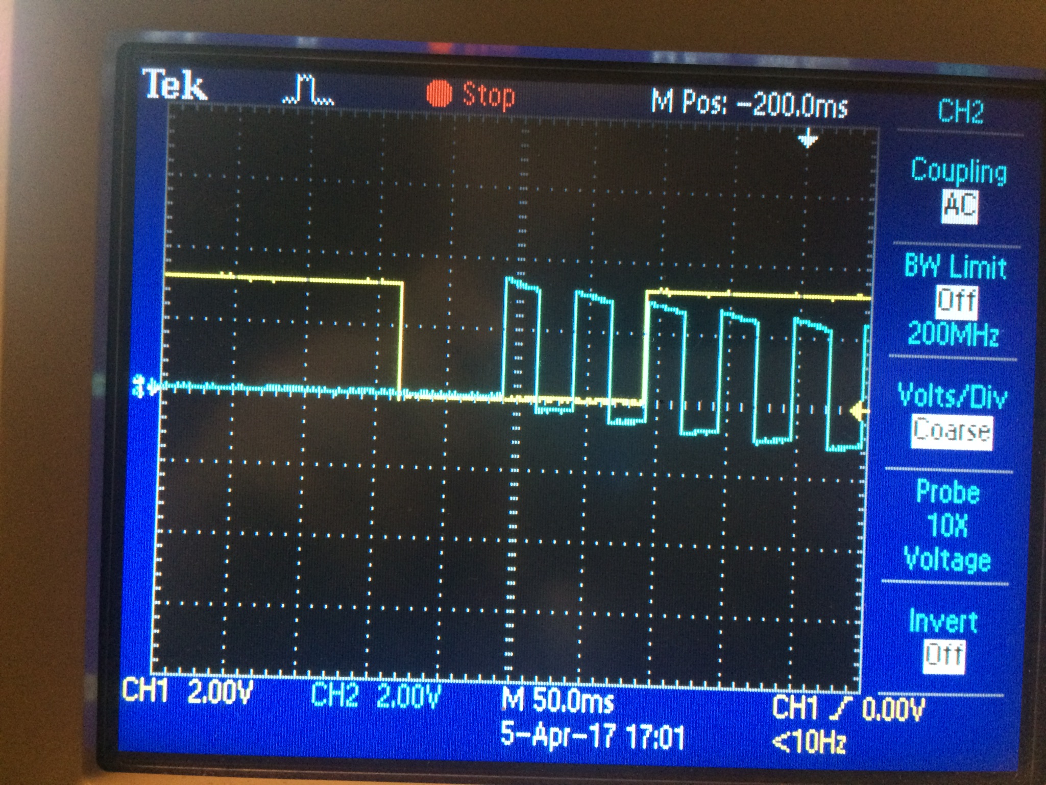
I put my device into DEEPSLEEP mode successfully. But then I can not recover the problem to work normally. 

Could you please help me find out the mistakes?

Here is my code:

static void deep_sleep_mode (void)
{

// Step 1: Active Self-refresh mode to DDR2
// Clear self refresh/low power (SR_PD) bit to 0
HWREG(SOC_DDR2_0_CTRL_REGS + DDR2_MDDR_SDRCR) &= ~DDR2_MDDR_SDRCR_SR_PD;
// Set the low power mode enable
HWREG(SOC_DDR2_0_CTRL_REGS + DDR2_MDDR_SDRCR) |= DDR2_MDDR_SDRCR_LPMODEN;

// Step 2: Disable PHY SATA, USB2.0, USB1.1

// Step 3: put PLL/PLLC0 and PLL/PLLC1 in bypass mode
/*PLLEN = 0 put pll in bypass mode in PLL0 */
HWREG(SOC_PLLC_0_REGS + PLLC_PLLCTL) &= ~PLLC_PLLCTL_PLLEN;
/*PLLEN = 0 put pll in bypass mode in PLL1 */
HWREG(SOC_PLLC_1_REGS + PLLC_PLLCTL) &= ~PLLC_PLLCTL_PLLEN;

// Step 4: Power down PLL 0 and PLL 1
/*PLLPWRDN = 1 in PLL0 */
HWREG(SOC_PLLC_0_REGS + PLLC_PLLCTL) |= PLLC_PLLCTL_PLLPWRDN;
/*PLLPWRDN = 1 in PLL1 */
HWREG(SOC_PLLC_1_REGS + PLLC_PLLCTL) |= PLLC_PLLCTL_PLLPWRDN;

// Step 5: Config DEEPSLEEP pin as Input only
// Config GP0[8] - DEEPSLEEP pin - pin number 9
uint32_t savePinmux = (HWREG(SOC_SYSCFG_0_REGS + SYSCFG0_PINMUX(0)) &
~(SYSCFG_PINMUX0_PINMUX0_31_28));
HWREG(SOC_SYSCFG_0_REGS + SYSCFG0_PINMUX(0)) =
(PINMUX0_GPIO0_8_ENABLE | savePinmux);
// Config this pin as input-only
GPIODirModeSet(SOC_GPIO_0_REGS, 9, GPIO_DIR_INPUT);

// Step 6: Config delay in the SLEEPCOUNT bit (ex: 0x0F)
HWREG(SOC_SYSCFG_1_REGS + SYSCFG1_DEEPSLEEP) |= (0x0F & SYSCFG1_DEEPSLEEP_SLEEPCOUNT);

// Step 7: set SLEEPENABLE bit in DEEPSLEEP to 1
HWREG(SOC_SYSCFG_1_REGS + SYSCFG1_DEEPSLEEP) |= SYSCFG1_DEEPSLEEP_SLEEPENABLE;

// Step 8: polling bit SLEEPCOMPLETE
while (~(SYSCFG1_DEEPSLEEP_SLEEPCOMPLETE &
HWREG(SOC_SYSCFG_1_REGS + SYSCFG1_DEEPSLEEP)))
{

}

// Step 9: Drive the DEEPSLEEP pin low

/***************************EXIT DEEPSLEEP MODE*****************************/

// Step 10: clear SLEEPENABLE bit in DEEPSLEEP to 0
HWREG(SOC_SYSCFG_1_REGS + SYSCFG1_DEEPSLEEP) &= ~SYSCFG1_DEEPSLEEP_SLEEPENABLE;

// Step 11: initialize PLL again
/* Clear PLLRST bit in PLLCTL to 0 */
HWREG(SOC_PLLC_0_REGS + PLLC_PLLCTL) &= ~PLLC_PLLCTL_PLLRST;
HWREG(SOC_PLLC_1_REGS + PLLC_PLLCTL) &= ~PLLC_PLLCTL_PLLRST;
/* Clear PLLPWRDN bit in PLLCTL*/
HWREG(SOC_PLLC_0_REGS + PLLC_PLLCTL) &= ~PLLC_PLLCTL_PLLPWRDN;
HWREG(SOC_PLLC_1_REGS + PLLC_PLLCTL) &= ~PLLC_PLLCTL_PLLPWRDN;
/* Set PLLRST bit in PLLCTL to 1 - out of reset*/
HWREG(SOC_PLLC_0_REGS + PLLC_PLLCTL) |= PLLC_PLLCTL_PLLRST;
HWREG(SOC_PLLC_1_REGS + PLLC_PLLCTL) |= PLLC_PLLCTL_PLLRST;
/* Wait for PLL to lock*/
/* Wait for 300 counts*/
Delay (300);
/*Set the PLLEN bit in PLLCTL to 1 - remove bypass mode*/
HWREG(SOC_PLLC_0_REGS + PLLC_PLLCTL) |= PLLC_PLLCTL_PLLEN;
HWREG(SOC_PLLC_1_REGS + PLLC_PLLCTL) |= PLLC_PLLCTL_PLLEN;

// Step 12: Enable clock DDR
/* Enable clock to SDRAM */
PSCModuleControl(SOC_PSC_1_REGS, HW_PSC_DDR2_MDDR, 0,PSC_MDCTL_NEXT_ENABLE);
/* Set RESET_PHY bit in DDR PHY*/
HWREG(SOC_DDR2_0_CTRL_REGS + DDR2_MDR_DRPYCRC) = DDR2_MDDR_DRPYRCR_RESET_PHY;
/* Clear MCLKSTOPEN bit in SDRCR*/
HWREG(SOC_DDR2_0_CTRL_REGS + DDR2_MDDR_SDRCR) &= ~DDR2_MDDR_SDRCR_MCLKSTOPEN;
/* Disable Self refresh rate */
// clear the low power mode
HWREG(SOC_DDR2_0_CTRL_REGS + DDR2_MDDR_SDRCR) &= ~DDR2_MDDR_SDRCR_LPMODEN;

}

Regards, Nghia Quy

  • Hi Nguyen,

    I've forwarded this to the experts. Their feedback should be posted here.

    BR
    Tsvetolin Shulev
  • Some guesses while the experts are thinking.

    Your sleepcount line:

    HWREG(SOC_SYSCFG_1_REGS + SYSCFG1_DEEPSLEEP) |= (0x0F & SYSCFG1_DEEPSLEEP_SLEEPCOUNT);

    may result in a sleepcount of 0xFFFF as the reset value is 0xFFFF. The sleepcount bits are not cleared before setting. Something like this:

    HWREG(SOC_SYSCFG_1_REGS + SYSCFG1_DEEPSLEEP) =
    ((HWREG(SOC_SYSCFG_1_REGS + SYSCFG1_DEEPSLEEP) & ~SYSCFG1_DEEPSLEEP_SLEEPCOUNT) | 0x000F);

    I assume your code is looping for SLEEPCOMPLETE. You should mux in DEEPSLEEP rather than GP0[8]. Skip GP0[8] code. Oddly, the StarterWare header does not define a constant for pinmux deepsleep. Use DEFAULT.

    uint32_t savePinmux = (HWREG(SOC_SYSCFG_0_REGS + SYSCFG0_PINMUX(0)) &
    ~(SYSCFG_PINMUX0_PINMUX0_31_28));
    HWREG(SOC_SYSCFG_0_REGS + SYSCFG0_PINMUX(0)) =
    (SYSCFG_PINMUX0_PINMUX0_31_28_DEFAULT<<SYSCFG_PINMUX0_PINMUX0_31_28_SHIFT | savePinmux);

    I suggest putting your code into L2 RAM(DSP) or L3 RAM(ARM) to separate deep sleep problems from DDR wakeup problems.

    You have two threads on this subject. The other one here:
    e2e.ti.com/.../585264

    Leave it to the moderators to sort out.
  • Hi Norman,

    Thanks for your answer, it is very helpful.
    1. About sleepcount, you are right, I fixed my code.
    2. About GP0[8]: I did the same your way, then I checked by view GPIO register when debugging by JTAG.
    3. I Put my code to Share_RAM area by using #pragma, then I checked by viewing the .map file

    The program still can not wake up after into DeepSleep mode.

    Now, I trying to check the processes turn off then turn on of PLL0/1 is right or not.
    The result is after turn off PLL 0/1, I guess this process is successful because the current consumtion did decrease dramatically.
    Then I try to turn on PLL 0/1, but after setting PLLEN bit in PLLCTL, the program will not do anything, it jump to unknown address 0xFFFF0010.

    I don't know why. Could you please help me to fix this error?
    I am using SYS/BIOS and here is my code test (only turn off PLL then turn on PLL):
    static void deep_sleep_mode (void)
    {
    // Turn off PLL
    /*PLLEN = 0 put pll in bypass mode in PLL0 */
    HWREG(SOC_PLLC_0_REGS + PLLC_PLLCTL) &= ~PLLC_PLLCTL_PLLEN;
    /*PLLEN = 0 put pll in bypass mode in PLL1 */
    HWREG(SOC_PLLC_1_REGS + PLLC_PLLCTL) &= ~PLLC_PLLCTL_PLLEN;

    Delay(4);

    // Step 4: Power down PLL 0 and PLL 1
    /*PLLPWRDN = 1 in PLL0 */
    HWREG(SOC_PLLC_0_REGS + PLLC_PLLCTL) |= PLLC_PLLCTL_PLLPWRDN;
    /*PLLPWRDN = 1 in PLL1 */
    HWREG(SOC_PLLC_1_REGS + PLLC_PLLCTL) |= PLLC_PLLCTL_PLLPWRDN;


    /***************************EXIT DEEPSLEEP MODE*****************************/

    // Turn on PLL
    /* Clear PLLRST bit in PLLCTL to 0 */
    HWREG(SOC_PLLC_0_REGS + PLLC_PLLCTL) &= ~PLLC_PLLCTL_PLLRST;
    /* Set PLL disable output*/
    HWREG(SOC_PLLC_0_REGS + PLLC_PLLCTL) |= PLLC_PLLCTL_PLLDIS;
    /* Clear PLLPWRDN bit in PLLCTL*/
    HWREG(SOC_PLLC_0_REGS + PLLC_PLLCTL) &= ~PLLC_PLLCTL_PLLPWRDN;
    /* Enable Toggle*/
    HWREG(SOC_PLLC_0_REGS + PLLC_PLLCTL) &= ~PLLC_PLLCTL_PLLDIS;
    /* Wait for 300 counts*/
    Delay (300);
    /* Set PLLRST bit in PLLCTL to 1 - out of reset*/
    HWREG(SOC_PLLC_0_REGS + PLLC_PLLCTL) |= PLLC_PLLCTL_PLLRST;
    /* Wait for 400 counts*/
    Delay (400);
    /*Set the PLLEN bit in PLLCTL to 1 - remove bypass mode*/
    HWREG(SOC_PLLC_0_REGS + PLLC_PLLCTL) |= PLLC_PLLCTL_PLLEN;
    // The program will jump to unknown address

    /* Clear PLLRST bit in PLLCTL to 0 */
    HWREG(SOC_PLLC_1_REGS + PLLC_PLLCTL) &= ~PLLC_PLLCTL_PLLRST;
    /* Set PLL disable output*/
    HWREG(SOC_PLLC_1_REGS + PLLC_PLLCTL) |= PLLC_PLLCTL_PLLDIS;
    /* Clear PLLPWRDN bit in PLLCTL*/
    HWREG(SOC_PLLC_1_REGS + PLLC_PLLCTL) &= ~PLLC_PLLCTL_PLLPWRDN;
    /* Enable Toggle*/
    HWREG(SOC_PLLC_1_REGS + PLLC_PLLCTL) &= ~PLLC_PLLCTL_PLLDIS;
    /* Wait for 300 counts*/
    Delay (300);
    /* Set PLLRST bit in PLLCTL to 1 - out of reset*/
    HWREG(SOC_PLLC_1_REGS + PLLC_PLLCTL) |= PLLC_PLLCTL_PLLRST;
    /* Wait for PLL to lock*/
    /* Wait for 400 counts*/
    Delay (400);
    /*Set the PLLEN bit in PLLCTL to 1 - remove bypass mode*/
    HWREG(SOC_PLLC_1_REGS + PLLC_PLLCTL) |= PLLC_PLLCTL_PLLEN;

    }
  • At one time, I did manage to place C6748 into deep sleep with other power saving. Wakeup via RTC because my board did not expose the DEEPSLEEP pin. That was with bare metal StarterWare. No experience with SYSBIOS. One would expect that sort of thing to be built. Hopefully SYSBIOS experts can comment.

    It is not clear from your last post about the which pin you have mux'ed in. Do not mux to the GPIO controller. Use the DEEPSLEEP connection. If I am reading your post correctly,
    - you successfully put the processor into the deep sleep state
    - you successfully woke the processor via the deepsleep pin, ie. exit looping on sleepcomplete bit
    - you are having problems restarting the PLL
    In theory, you could leave the PLL as is and continue executing with a very slow clock. SYSBIO timers and scheduling probably would not like it.

    PLL config is quite tricky. I'll have to review my notes and get back to you if I find anything.
  • Your PLL code might be missing a clear of PLLENSRC before PLLEN is modified. Also you may have to unlock the PLL registers. See CFGCHIP0:PLL_MASTER_LOCK and CFGCHIP3:PLL1_MASTER_LOCK.
  • Hi Norman,

    Thank for your feedback.

    I fixed the PLL configure error, it related about waiting cycles when changing PLLEN bit.

    I see that, my program stucks in polling loop SLEEPCOMPLETE bit. Then I changed my configurations for PINMUX0 is to DEEPSLEEP (not GPIO input), but the program still stucks in while loop.

    Here is my configuration DEEPSLEEP pin and the loop:

    #define PINMUX0_31_28_DEEPSLEEP (0x0FFFFFFF)

    // Config GP0[8] - DEEPSLEEP pin - pin number 9
    savePinMux = HWREG(SOC_SYSCFG_0_REGS + SYSCFG0_PINMUX(0));
    HWREG(SOC_SYSCFG_0_REGS + SYSCFG0_PINMUX(0)) = PINMUX0_31_28_DEEPSLEEP & savePinMux;
    // Step 6: Config delay in the SLEEPCOUNT bit (ex: 0x0F)
    HWREG(SOC_SYSCFG_1_REGS + SYSCFG1_DEEPSLEEP) = \
    ((HWREG(SOC_SYSCFG_1_REGS + SYSCFG1_DEEPSLEEP) &
    ~SYSCFG1_DEEPSLEEP_SLEEPCOUNT) | 0x000F);

    // Step 7: set SLEEPENABLE bit in DEEPSLEEP to 1
    HWREG(SOC_SYSCFG_1_REGS + SYSCFG1_DEEPSLEEP) |= SYSCFG1_DEEPSLEEP_SLEEPENABLE;

    // Step 8: polling bit SLEEPCOMPLETE
    do
    {
    awake = SYSCFG1_DEEPSLEEP_SLEEPCOMPLETE & HWREG(SOC_SYSCFG_1_REGS + SYSCFG1_DEEPSLEEP);
    }
    while (0 == awake);

    HWREG(SOC_SYSCFG_1_REGS + SYSCFG1_DEEPSLEEP) &= ~SYSCFG1_DEEPSLEEP_SLEEPENABLE;

    Do I have any mistake here?

    Thanks you so much,

    Nghia Quy

  • The pinmux code depends on the reset value of PINMUX0 being zero. Which it should be but just in case:

    savePinmux = (HWREG(SOC_SYSCFG_0_REGS + SYSCFG0_PINMUX(0))
    savePinmux &= ~(SYSCFG_PINMUX0_PINMUX0_31_28));
    savePinmux |= (SYSCFG_PINMUX0_PINMUX0_31_28_DEFAULT<<SYSCFG_PINMUX0_PINMUX0_31_28_SHIFT);
    HWREG(SOC_SYSCFG_0_REGS + SYSCFG0_PINMUX(0)) = savePinmux;

    Just to check, which pad are do trying to toggle for enter/exit sleep? Otherwise, it should work.
  • Thank for your quick reply, But, i think i do not really understand your idea. Do you mean I should use your code block instead of mine: // Config GP0[8] - DEEPSLEEP pin - pin number 9 savePinMux = HWREG(SOC_SYSCFG_0_REGS + SYSCFG0_PINMUX(0)); HWREG(SOC_SYSCFG_0_REGS + SYSCFG0_PINMUX(0)) = PINMUX0_31_28_DEEPSLEEP & savePinMux; // Step 6: Config delay in the SLEEPCOUNT bit (ex: 0x0F) I will test and feedback to you asap. And your question "which part are do trying to toggle for enter/exit sleep?" Do you mean arm or dsp part? I use both parts so I am trying controller all of them to deepsleep then exit this mode. Thank again, Nghia Quy
  • Sorry, my eyes missed the first zero in definition of PINMUX0_31_28_DEEPSLEEP. That would indeed mean field PINMUX0_31_28 is set to zero.

    The PAD number is F4 which is multiplexed RTC_ALARM/GP0[8]/UART2_CTS/DEEPSLEEP. On the LCDK, this pad is not connected. I assume that you are using a custom board and that you have not used the pad for one of the other functions. Documentation says the DEEPSLEEP pin is normally high, active low.
  • Hi Norman,

    I am using a custom board and I only use F4 pin for Deepsleep function.
    Normally, this pin is high, it only changes to low status when setting DeepSleep.

    I really do not understand why the program do not exit the while loop. The configuration is so clear and logical.
    When you used C6748, did you use JTAG for debug?
    I am using JTAG, but the board can not keep the connection to CCS right after Deepsleep pin being low. So I can not debug the status of board after into deepsleep mode (even then the deepsleep pin changed to high level).
    Did you miss the issue like me?

    Thank you,
    Nghia Quy
  • Hi Tsvetolin Shulev,

    I am still waiting for the feedback from your experts.
    This is a critical issue.
    So please help me resolve this issue.

    Best Regards,
    Nghia Quy
  • Hi Norman,

    In TI docs, part 10.10.3 Deep SleepSequence:
    Step 5. The DEEPSLEEP pin is driven high and the on-chip oscillator is enabled.

    Could you help me answer some questions?
    What is the on-chip oscillator? and do I need configure registers for enable on-chip oscillator?
  • Hi 

    You will see on chip oscillator mentioned in the TRM and datasheet as either internal oscillator or crystal oscillator. There are no registers needed to enable this.

    you can set the PLLCTRL register bit CLKMODE to 1, but overall this should not have any impact on your deep sleep functionality (just very minor impact on power) 

  • Going back to the issue at hand.. it is hard to do code audit on what may be going wrong with your code and/or your custom board in terms of DEEPSLEEP pin handling.

    Perhaps you can try to see if using RTC alarm , allows the same code you have to recover from deep sleep reliably.
    To keep this simple - you should try to do this with
    1) testing this in device power on default state, where PLLs are bypassed etc
    2) keeping everything in internal memory ( i believe you are doing this now following Norman's suggestion)
    3) Waking up from deepsleep but w/o reconfiguring PLLs.

    ---
    Here is some old code snippet, that i believe should be good enough to going into deepsleep and recovering from it via RTC alarm... this may help

    ---
    #if defined(__TMS470__)
    #define TARGET_ISA 'A' //ARM926EJ
    #elif defined(_TMS3206X)
    #define TARGET_ISA 'D' //C64x
    #endif

    #define PDCCMD_REG *(Uint32 volatile *)0x01810000

    /*PLL0 Controller Control Register */
    #define PLL0_BASE_ADDR 0x01C11000
    #define PLL0_PLLCTL (PLL0_BASE_ADDR + 0x100) /*PLL Control Register*/
    #define PLL0_OCSEL (PLL0_BASE_ADDR + 0x104) /*OBSCLK Select Register*/
    #define PLL0_SECCTL (PLL0_BASE_ADDR + 0x108) /*PLL Secondary Control Register*/
    #define PLL0_PLLM (PLL0_BASE_ADDR + 0x110) /*PLL Multiplier Control Register*/
    #define PLL0_PREDIV (PLL0_BASE_ADDR + 0x114) /*PLL Pre-Divider control Register*/
    #define PLL0_PLLDIV1 (PLL0_BASE_ADDR + 0x118) /*PLL Controller Div1 Register*/
    #define PLL0_PLLDIV2 (PLL0_BASE_ADDR + 0x11C) /*PLL Controller Div2 Register*/
    #define PLL0_PLLDIV3 (PLL0_BASE_ADDR + 0x120) /*PLL Controller Div3 Register*/
    #define PLL0_OSCDIV1 (PLL0_BASE_ADDR + 0x124) /*Oscilator Divider Register*/
    #define PLL0_POSTDIV (PLL0_BASE_ADDR + 0x128) /*PLL Post-Divider Register*/
    #define PLL0_BPDIV (PLL0_BASE_ADDR + 0x12C) /*Bypass Divider Register*/
    #define PLL0_WAKEUP (PLL0_BASE_ADDR + 0x130) /*Wakeup Register*/
    #define PLL0_PLLCMD (PLL0_BASE_ADDR + 0x138) /*PLL Controller Command Register*/
    #define PLL0_PLLSTAT (PLL0_BASE_ADDR + 0x13C) /*PLL Controller Status Register*/
    #define PLL0_ALNCTL (PLL0_BASE_ADDR + 0x140) /*PLL Controller Clock Align Control Register*/
    #define PLL0_DCHANGE (PLL0_BASE_ADDR + 0x144) /*PLLDiv Ratio Change status Register*/
    #define PLL0_CKEN (PLL0_BASE_ADDR + 0x148) /*Clock Enable Control Register*/
    #define PLL0_CKSTAT (PLL0_BASE_ADDR + 0x14C) /*Clock Status Register*/
    #define PLL0_SYSTAT (PLL0_BASE_ADDR + 0x150) /*SYSCLK Status Register*/
    #define PLL0_PLLDIV4 (PLL0_BASE_ADDR + 0x160) /*PLL Controller Div4 Register*/
    #define PLL0_PLLDIV5 (PLL0_BASE_ADDR + 0x164) /*PLL Controller Div5 Register*/
    #define PLL0_PLLDIV6 (PLL0_BASE_ADDR + 0x168) /*PLL Controller Div6 Register*/
    #define PLL0_PLLDIV7 (PLL0_BASE_ADDR + 0x16C) /*PLL Controller Div7 Register*/
    #define PLL0_PLLDIV8 (PLL0_BASE_ADDR + 0x170) /*PLL Controller Div8 Register*/
    #define PLL0_PLLDIV9 (PLL0_BASE_ADDR + 0x174) /*PLL Controller Div8 Register*/

    /*PLL1 Controller Control Register */
    #define PLL1_BASE_ADDR 0x01E1A000
    #define PLL1_PLLCTL (PLL1_BASE_ADDR + 0x100) /*PLL Control Register*/
    #define PLL1_OCSEL (PLL1_BASE_ADDR + 0x104) /*OBSCLK Select Register*/
    #define PLL1_SECCTL (PLL1_BASE_ADDR + 0x108) /*PLL Secondary Control Register*/
    #define PLL1_PLLM (PLL1_BASE_ADDR + 0x110) /*PLL Multiplier Control Register*/
    #define PLL1_PREDIV (PLL1_BASE_ADDR + 0x114) /*PLL Pre-Divider control Register*/
    #define PLL1_PLLDIV1 (PLL1_BASE_ADDR + 0x118) /*PLL Controller Div1 Register*/
    #define PLL1_PLLDIV2 (PLL1_BASE_ADDR + 0x11C) /*PLL Controller Div2 Register*/
    #define PLL1_PLLDIV3 (PLL1_BASE_ADDR + 0x120) /*PLL Controller Div3 Register*/
    #define PLL1_OSCDIV1 (PLL1_BASE_ADDR + 0x124) /*Oscilator Divider Register*/
    #define PLL1_POSTDIV (PLL1_BASE_ADDR + 0x128) /*PLL Post-Divider Register*/
    #define PLL1_BPDIV (PLL1_BASE_ADDR + 0x12C) /*Bypass Divider Register*/
    #define PLL1_WAKEUP (PLL1_BASE_ADDR + 0x130) /*Wakeup Register*/
    #define PLL1_PLLCMD (PLL1_BASE_ADDR + 0x138) /*PLL Controller Command Register*/
    #define PLL1_PLLSTAT (PLL1_BASE_ADDR + 0x13C) /*PLL Controller Status Register*/
    #define PLL1_ALNCTL (PLL1_BASE_ADDR + 0x140) /*PLL Controller Clock Align Control Register*/
    #define PLL1_DCHANGE (PLL1_BASE_ADDR + 0x144) /*PLLDiv Ratio Change status Register*/
    #define PLL1_CKEN (PLL1_BASE_ADDR + 0x148) /*Clock Enable Control Register*/
    #define PLL1_CKSTAT (PLL1_BASE_ADDR + 0x14C) /*Clock Status Register*/
    #define PLL1_SYSTAT (PLL1_BASE_ADDR + 0x150) /*SYSCLK Status Register*/
    #define PLL1_PLLDIV4 (PLL1_BASE_ADDR + 0x160) /*PLL Controller Div4 Register*/
    #define PLL1_PLLDIV5 (PLL1_BASE_ADDR + 0x164) /*PLL Controller Div5 Register*/
    #define PLL1_PLLDIV6 (PLL1_BASE_ADDR + 0x168) /*PLL Controller Div6 Register*/
    #define PLL1_PLLDIV7 (PLL1_BASE_ADDR + 0x16C) /*PLL Controller Div7 Register*/
    #define PLL1_PLLDIV8 (PLL1_BASE_ADDR + 0x170) /*PLL Controller Div8 Register*/
    #define PLL1_PLLDIV9 (PLL1_BASE_ADDR + 0x174) /*PLL Controller Div8 Register*/

    /*SYSCFG0 Register */
    #define SYSCFG0_BASE_ADDR 0x01C14000
    #define SYSCFG0_KICK0 (SYSCFG0_BASE_ADDR + 0x38) /*KICK0 register*/
    #define SYSCFG0_KICK1 (SYSCFG0_BASE_ADDR + 0x3C) /*KICK1 register*/
    #define SYSCFG0_PINMUX0 (SYSCFG0_BASE_ADDR + 0x120) /*PINMUX0 register*/

    /*SYSCFG1 Register */
    #define SYSCFG1_BASE_ADDR 0x01E2C000
    #define SYSCFG1_DDRSLEW (SYSCFG1_BASE_ADDR + 0x04)
    #define SYSCFG1_DEEPSLEEP (SYSCFG1_BASE_ADDR + 0x08)
    #define SYSCFG1_PUPDEN (SYSCFG1_BASE_ADDR + 0x0C)
    #define SYSCFG1_PUPDSEL (SYSCFG1_BASE_ADDR + 0x10)
    #define SYSCFG1_RXACTIVE (SYSCFG1_BASE_ADDR + 0x14)

    /*RTC Register */
    #define RTC_BASE_ADDR 0x01C23000
    #define RTC_SECOND (RTC_BASE_ADDR + 0x00)
    #define RTC_MINUTE (RTC_BASE_ADDR + 0x04)
    #define RTC_HOUR (RTC_BASE_ADDR + 0x08)
    #define RTC_DAY (RTC_BASE_ADDR + 0x0C)
    #define RTC_MONTH (RTC_BASE_ADDR + 0x10)
    #define RTC_YEAR (RTC_BASE_ADDR + 0x14)
    #define RTC_DOTW (RTC_BASE_ADDR + 0x18)
    #define RTC_ALMSEC (RTC_BASE_ADDR + 0x20)
    #define RTC_CTRL (RTC_BASE_ADDR + 0x40)
    #define RTC_STATUS (RTC_BASE_ADDR + 0x44)
    #define RTC_INTR (RTC_BASE_ADDR + 0x48)
    #define RTC_OSC (RTC_BASE_ADDR + 0x54)
    #define RTC_KICK0R (RTC_BASE_ADDR + 0x6C)
    #define RTC_KICK1R (RTC_BASE_ADDR + 0x70)

    /*TIMER Register */
    #define TMR_BASE_ADDR 0x01C20000
    #define TMR_TIM12 (TMR_BASE_ADDR + 0x10)
    #define TMR_PRD12 (TMR_BASE_ADDR + 0x18)
    #define TMR_TCR (TMR_BASE_ADDR + 0x20)
    #define TMR_TGCR (TMR_BASE_ADDR + 0x24)

    /*Extra variables */
    #define RTC_RESET_TIME 2288

    unsigned int main()
    {
    unsigned int counter;

    /**** CONFIGURING DEEPSLEEP ****/
    //1. DDR2/mDDR should be clock gated
    // --No configuration needed. Default clock gated

    //2. SATA PHY should be disabled
    // --No configuration needed. Default disabled

    //3. USB2.0 PHY should be disabled
    // --No configuration needed. Default disabled

    //4. USB1.1 PHY should be disabled
    // --No configuration needed. Default disabled

    //5. PLLs should be placed in bypass mode (clear PLLEN bit in PLLCTL register)
    // --No configuration needed. Default in bypass mode

    //6. PLLs should be powered down (set PLLPWRDN bit in PLLCTL register)
    // --No configuration needed. Default powered down

    //7. Configure the desired wake-up time as an alarm in RTC
    *(unsigned int*) TMR_TIM12 = 0x00000000;
    *(unsigned int*) TMR_PRD12 = 0xFFFFFFFF;
    *(unsigned int*) TMR_TGCR = (*(unsigned int*) TMR_TGCR & ~0x000C) | 0x0004; // Dual, unchained mode
    *(unsigned int*) TMR_TGCR = (*(unsigned int*) TMR_TGCR & ~0x0001) | 0x0001; // Not in reset
    *(unsigned int*) TMR_TCR = (*(unsigned int*) TMR_TCR & ~0x00C0) | 0x0080; // Enabled continuously

    *(unsigned int*) RTC_KICK0R = 0x83E70B13; //Unlock RTC registers
    *(unsigned int*) RTC_KICK1R = 0x95A4F1E0;

    *(unsigned int*) RTC_OSC = (*(unsigned int*) RTC_OSC & ~0x0020) | 0x0020; // Software reset
    counter = *(unsigned int*) TMR_TIM12 + RTC_RESET_TIME;
    while( *(unsigned int*) TMR_TIM12 < counter ){}

    *(unsigned int*) RTC_ALMSEC = *(unsigned int*) RTC_ALMSEC | 0x0015; //Set the alarm (15 seconds)
    *(unsigned int*) RTC_INTR = *(unsigned int*) RTC_INTR | 0x0008; //Enable Alarm

    *(unsigned int*) RTC_CTRL = *(unsigned int*) RTC_CTRL | 0x0081; //Enable split power and start RTC

    //while((*(unsigned int*) RTC_STATUS & 0x0040) == 0){} // Extra code to test the alarm

    //8. Configure PINMUX0_31_28 as output of RTC_ALARM.
    *(unsigned int*) SYSCFG0_KICK0 = 0x83E70B13;
    *(unsigned int*) SYSCFG0_KICK1 = 0x95A4F1E0;
    *(unsigned int*) SYSCFG0_PINMUX0 = *(unsigned int*) SYSCFG0_PINMUX0 & ~0xF0000000;
    *(unsigned int*) SYSCFG0_PINMUX0 = *(unsigned int*) SYSCFG0_PINMUX0 | 0x20000000;

    //9. Configure the desired delay in SLEEPCOUNT
    *(unsigned int*) SYSCFG1_DEEPSLEEP = *(unsigned int*) SYSCFG1_DEEPSLEEP & ~0xFFFF; // Set sleepcount to 0

    //10. Set the SLEEPENABLE bit in DEEPSLEEP. Automatically clears the SLEEPCOMPLETE bit.
    *(unsigned int*) SYSCFG1_DEEPSLEEP = *(unsigned int*) SYSCFG1_DEEPSLEEP | 0x80000000; // Enable deepsleep

    //11. Begin polling SLEEPCOMPLETE until it is set to 1 (set once device is woken up)
    while((*(unsigned int*) SYSCFG1_DEEPSLEEP & 0x40000000) == 0){} // Wait for the device to come out of deepsleep

    //12. Clear the SLEEPENABLE bit in DEEPSLEEP
    *(unsigned int*) SYSCFG1_DEEPSLEEP = *(unsigned int*) SYSCFG1_DEEPSLEEP & ~0x80000000; // Disable deepsleep

    asm(" IDLE");

    //should never reach here
    return (1);
    }
    -----
  • Additionally there were some questions on SYSBIOS etc.
    We still do have the PWRM module under sysbios that show cases some of the sleep modes , as part of the release there will be additional code in the pmi/psc libraries, that you may be able to use as reference.

    processors.wiki.ti.com/.../Power_Module_for_C6748_and_OMAP-L138
  • It's been about 5 years since I experimented with the deep sleep feature on a C6748 LCDK. I vaguely remember the JTAG does go down and CCS really hates that. I had to reset the board and restart CCS to recover. Later, I found I could use "Run->Free Run" to remain connected. That meant no single stepping though code. I depended on the UART and GPIOs to tell me the progress of the sleep.

    Did you try commenting out the SLEEPCOMPLETE loop to check that the wakeup code is good?
  • @Norman: Thanks for your answer, I tried commenting out the SLEEPCOMPLETE loop and the wake up process is good.

    @Mukul: Thanks for your feedback, I will try to test your sample code, but RTC is not available in my current hardware now, so I need to have a little time to modify my board.

    Today, I try to test a sample code to check DEEPSLEEP functions.

    My hardware includes:

    • A button connected to DEEPSLEEP pin (GP0[8]), it is high default.
    • A pin GP6[14] is output pin to debug

    My software process is:

    • I press the button to enable DEEPSLEEP mode, then I release for waking up and put an pulse continuously in GP6[14]
    • If the program wakes up from DEEPSLEEP mode, it will have a square pulse in GP6[14] pin.

    And the result is:

    1. Most of times, the program did not wake up from DEEPSLEEP mode
    2. In sometimes, if I pressed then released really fast the button, the program will wake up and having a pulse in GP6[14]
    3. But I viewed on oscilloscope then I saw that having a pulse in GP6[14] (blue line) before the level of DEEPSLEEP pin changing from low to high (yellow line). It means the program waked up before DEEPSLEEP pin changing from low to high. According the theory, it is not possible.

    Anyone can help me understand this results?

    I attached .cmd and source file for your debugging.

    /**
     * \file    gpioCardDetect.c
     *
     * \brief   This is a sample application file demonstrating the use of
     *          a GPIO pin to generate an interrupt whenever an MMC/SD card
     *          is inserted or ejected from the Evaluation Module(EVM).
     */
    
    /*
    * Copyright (C) 2012 Texas Instruments Incorporated - http://www.ti.com/ 
    *
    *  Redistribution and use in source and binary forms, with or without 
    *  modification, are permitted provided that the following conditions 
    *  are met:
    *
    *    Redistributions of source code must retain the above copyright 
    *    notice, this list of conditions and the following disclaimer.
    *
    *    Redistributions in binary form must reproduce the above copyright
    *    notice, this list of conditions and the following disclaimer in the 
    *    documentation and/or other materials provided with the   
    *    distribution.
    *
    *    Neither the name of Texas Instruments Incorporated nor the names of
    *    its contributors may be used to endorse or promote products derived
    *    from this software without specific prior written permission.
    *
    *  THIS SOFTWARE IS PROVIDED BY THE COPYRIGHT HOLDERS AND CONTRIBUTORS 
    *  "AS IS" AND ANY EXPRESS OR IMPLIED WARRANTIES, INCLUDING, BUT NOT 
    *  LIMITED TO, THE IMPLIED WARRANTIES OF MERCHANTABILITY AND FITNESS FOR
    *  A PARTICULAR PURPOSE ARE DISCLAIMED. IN NO EVENT SHALL THE COPYRIGHT 
    *  OWNER OR CONTRIBUTORS BE LIABLE FOR ANY DIRECT, INDIRECT, INCIDENTAL, 
    *  SPECIAL, EXEMPLARY, OR CONSEQUENTIAL DAMAGES (INCLUDING, BUT NOT 
    *  LIMITED TO, PROCUREMENT OF SUBSTITUTE GOODS OR SERVICES; LOSS OF USE,
    *  DATA, OR PROFITS; OR BUSINESS INTERRUPTION) HOWEVER CAUSED AND ON ANY
    *  THEORY OF LIABILITY, WHETHER IN CONTRACT, STRICT LIABILITY, OR TORT 
    *  (INCLUDING NEGLIGENCE OR OTHERWISE) ARISING IN ANY WAY OUT OF THE USE 
    *  OF THIS SOFTWARE, EVEN IF ADVISED OF THE POSSIBILITY OF SUCH DAMAGE.
    */
    
    #include "gpio.h"
    #include "psc.h"
    
    #include "lcdkOMAPL138.h"
    
    // Test Deep sleep mode
    #include "hw_ddr2_mddr.h"
    /* Device/Platform lib headers */
    #include "soc_OMAPL138.h"
    #include "hw_types.h"
    #include "hw_pllc_OMAPL138.h"
    #include "hw_syscfg0_OMAPL138.h"
    #include "hw_syscfg1_OMAPL138.h"
    #include "gpio.h"
    #include "psc.h"
    #include "stdio.h"
    
    
    #define PINMUX0_31_28_GPIO (0x80000000)
    /* Pin Multiplexing bit mask to select GP0[8] pin. */
    #define PINMUX0_31_28_DEEPSLEEP (0x0FFFFFFF)
    
    #define PINMUX13_CLKOUT_ENABLE    (SYSCFG_PINMUX13_PINMUX13_7_4_OBSCLK0  << SYSCFG_PINMUX13_PINMUX13_7_4_SHIFT)
    #define PINMUX13_GPIO_ENABLE    (SYSCFG_PINMUX13_PINMUX13_7_4_GPIO6_14 << SYSCFG_PINMUX13_PINMUX13_7_4_SHIFT)
    
    /****************************************************************************/
    /*              LOCAL FUNCTION PROTOTYPES                                   */
    /****************************************************************************/
    static void Delay(volatile unsigned int delay);
    /****************************************************************************/
    /*              GLOBAL VARIABLES                                            */
    /****************************************************************************/
    
    
    /****************************************************************************/
    /*             LOCAL FUNCTION DEFINITIONS                                   */
    /****************************************************************************/
    
    
    int main(void)
    {
        int savePinMux;
        static unsigned int deepsleep;
    
        /* The Local PSC number for GPIO is 3. GPIO belongs to PSC1 module.*/
        PSCModuleControl(SOC_PSC_1_REGS, HW_PSC_GPIO, PSC_POWERDOMAIN_ALWAYS_ON,
                                                             PSC_MDCTL_NEXT_ENABLE);
    
        // Config GP6[14] - as out pin
        savePinMux = (HWREG(SOC_SYSCFG_0_REGS + SYSCFG0_PINMUX(13)) &
                                                   ~(SYSCFG_PINMUX13_PINMUX13_7_4));
        HWREG(SOC_SYSCFG_0_REGS + SYSCFG0_PINMUX(13)) =
                                              (PINMUX13_GPIO_ENABLE | savePinMux);
    
        GPIODirModeSet(SOC_GPIO_0_REGS, 111, GPIO_DIR_OUTPUT);
        GPIOPinWrite(SOC_GPIO_0_REGS, 111, GPIO_PIN_LOW);
    
        while(1)
        {
            // Config GP0[8] - DEEPSLEEP pin - pin number 9
            savePinMux = HWREG(SOC_SYSCFG_0_REGS + SYSCFG0_PINMUX(0));
            HWREG(SOC_SYSCFG_0_REGS + SYSCFG0_PINMUX(0)) = PINMUX0_31_28_DEEPSLEEP & savePinMux;
            // Step 6: Config delay in the SLEEPCOUNT bit (ex: 0x0F)
            HWREG(SOC_SYSCFG_1_REGS + SYSCFG1_DEEPSLEEP) = \
                                       ((HWREG(SOC_SYSCFG_1_REGS + SYSCFG1_DEEPSLEEP) &
                                               ~SYSCFG1_DEEPSLEEP_SLEEPCOUNT) | 0x0001);
    
            // Step 7: set SLEEPENABLE bit in DEEPSLEEP to 1
            HWREG(SOC_SYSCFG_1_REGS + SYSCFG1_DEEPSLEEP) |= SYSCFG1_DEEPSLEEP_SLEEPENABLE;
    
            // Step 8: polling bit SLEEPCOMPLETE
            while (0 == (SYSCFG1_DEEPSLEEP_SLEEPCOMPLETE & HWREG(SOC_SYSCFG_1_REGS + SYSCFG1_DEEPSLEEP)))
            {
            }
    
            HWREG(SOC_SYSCFG_1_REGS + SYSCFG1_DEEPSLEEP) &= ~SYSCFG1_DEEPSLEEP_SLEEPENABLE;
    
            while (1)
            {
                Delay(0xFFFF);
                GPIOPinWrite(SOC_GPIO_0_REGS, 111, GPIO_PIN_HIGH);
                Delay(0xFFFF);
                GPIOPinWrite(SOC_GPIO_0_REGS, 111, GPIO_PIN_LOW);
            }
        }
    
    
    }
    
    /*
    ** \brief  This function checks the insertion status of the MMC/SD card
    **         in the device and prints related statements on the serial
    **         commuincation console of the external device.
    **         
    */
    
    /*
    ** \brief   This function can be called to generate a delay.
    */
    
    static void Delay(volatile unsigned int delay)
    {
        while(delay--);
    }
    
    /*****************************END OF FILE************************************/
    

  • Some comments, assuming DeepSleepTest.c is the complete test code:

    1) You can move the pinmux of DEEPSLEEP pin out of the loop.

    2) Your code DeepSleepTest.c does not have any PLL shutdown and restart. I believe you have to have that at a minimum. The deepsleep signal will gate the clock and the PLL will lose its reference clock. From what I have seen on the forum, the processor does not like a jittery PLL and tend to lock up. That might be what is happenning when your processor enters deepsleep. This is where commenting out your SLEEPCOMPLETE loop is a goot test of the PLL shutdown and restart without going into deepsleep. Same for DDR stop/start and any other PSC stop/start code.

    3) The apparent waking before the deepsleep signal is deasserted may be due to bounce on your switch. It is deasserting ever so briefly immediately after press the button. You might need to add a debounce resisitor/capacitor of some kind. I'm firmware and can't recommend a values or schematic.
  • Hi,

    Finally, I can do deepsleep mode in OMAP.
    You were right, in my code DeepSleepTest.c, I have to add PLL shutdown and restart.

    Thank Norman and Mukul Bhatnagar so much for your helps,

    Best Regards,
    Quy Nguyen
  • Thanks for updating the thread. Glad to hear that you are up and running.
    Appreciate the support Norman provided on this to set you on the right debug path.