This thread has been locked.

If you have a related question, please click the "Ask a related question" button in the top right corner. The newly created question will be automatically linked to this question.

[C6748] PLL Power Filtering

I have a question regarding external filtering on the PLL supply. The datasheet for TMS320C6748 says designers should filter the PLLs' ground with a bead.
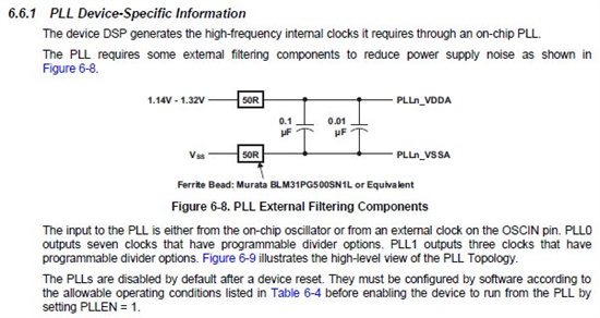

Is it right to have these grounds separated by a bead?  If there is a path between PLLn_VSSA and VSS on the DSP's silicon, high-frequency voltage noise across this path could be a problem.  The IC designer may keep grounds apart on the die but intend for the PCB designer to connect these together right at the part. 

If this case is different, can anyone tell me why?  It feels very weird to put an inductor on a ground line.  I clearly understand the desire to keep digital noise off the PLL ground, BUT in my experience grounds are fully isolated within the IC, so filtering the ground pin makes the noise worse.  I am open hearing how this case is different.

  • Charles Gervasi,

    The filtering that we put in the datasheet is what we recommend you to use, and this is what we stand behind for reliable operation. As you know, it costs more to use 2 inductors, just like it costs more to use 2 capacitors. You are certainly free to make your own engineering design decisions based on your knowledge and experience, and if your system has the reliability and noise-immunity that you want then all is good.

    Please also be aware that there are two sets of these filters required, one set of 2 beads + 2 caps for PLL0 and one set of 2 beads + 2 caps for PLL1.

    Regards,
    RandyP

  • RandyP said:
    As you know, it costs more to use 2 inductors, just like it costs more to use 2 capacitors.


    Of course.  I never said this is a cost issue.  I'm asking an engineering question.  Suppose there is noise on the digital ground, which I agree there will be.  Does filtering that noise help?  Filtering it means there will be an AC voltage across the path inside the IC from PLL ground to digital ground.  Is that a good thing?  Is the PLL ground isolated inside the IC from digital ground?  Is this a case of T&E plus recommendations from the IC designers showing that filtering ground works even though we're not completely clear why?

    Thank you for the note about there being separate beads and caps for the PLLs.  I didn't realize that.

    Thanks!

    CJ

  • Charles,

    The PLL VSSA grounds are routed within the package to dedicated pins with no internal connections to digital ground.  The use of bead filtering on VSSA is a recommendation provided by the PLL design team, which was then forwarded to the datasheet.

    -Tommy