This thread has been locked.
If you have a related question, please click the "Ask a related question" button in the top right corner. The newly created question will be automatically linked to this question.
Hi All,
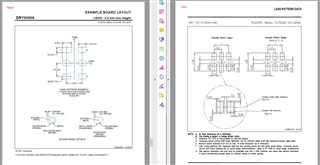
I have a question on TPD4S012.
The layout pattern has changed between the old and new datasheet versions.
Please tell us how the layout pattern was changed and the background.
Best Regards,
Ishiwata
Hi Ishiwata,
Thank you for reaching out. I have contacted our packaging team and will let you know when I get a response on this.
Regards,
Matt Smith
Hi Ishiwata,
The old datasheet was based on an old drawing, where the PCB pad dimension was 0.3 X 0.49mm.
The update drawing PCB pad size is 0.2 X 0.3mm which we confirmed is correct now.
Let me know if you have any more questions about this.
Regards,
Matt Smith
Hi Matt,
Thank you for your answer.
Please tell me the reason for the change.
Has the package changed?
Or was the wrong information included in the old datasheet?
Best Regards,
Ishiwata
Hi Shuji,
The package has not changed. The old datasheet just had incorrect information.
Regards,
Matt Smith